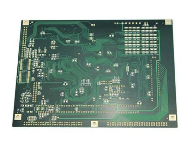
Flexible PCBs are used in demanding applications such as aerospace, satellites, IoT, medical, and wearable devices. They offer improved endurance to vibrations and high temperatures, making them more sustainable against harsh environmental conditions.
Flex PCB design requires a slightly different approach than rigid PCBs. While designing a flex board, you must consider the board outline, bending requirements, optimum material selection, stack-up, placement of copper features, and cost factors.
This article provides several useful pointers to ensure maximum reliability and manufacturability when planning your flex printed circuit.
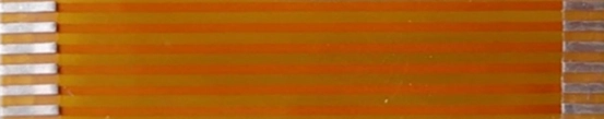
Detail 1. How to tell if an FPC is properly inserted?
One common issue we see in production is functional failure caused by incomplete FPC insertion.
The problem usually comes from the assembly process. On high-speed lines, operators may not consistently verify whether each FPC is fully inserted into the connector.
Key point
Key point: add a visual insertion marker on the design side. When the FPC reaches the correct position, the line aligns with the bottom edge of the ZIF connector. In that way, you know it’s fully inserted.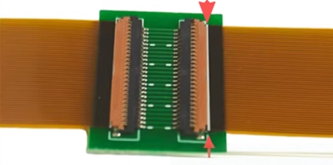
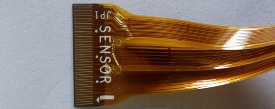
Detail 2. How to prevent reverse insertion on non-1:1 FPCs
Some FPCs have the same pin count on both ends, but the signals aren’t mapped 1:1. There are power and ground lines mixed in, Incorrect insertion can lead to overheating, functional failure, or even component burnout.
Key point
Key point: In addition to insertion alignment marks as mentioned above, print clear silkscreen markings on both sides of the FPC. Make sure the labels are large and easy to read.
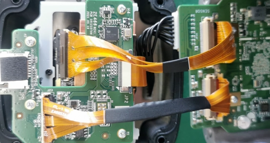
Detail 3. How to prevent damage when assembling wide FPCs
Wide FPCs can be tricky during assembly. When routing or bending them, it’s easy to cause damage, which directly impacts yield.
Key point
Key point: Break the design into smaller sections. For FPCs with a large number of pins and wide layouts, you can leave an empty area in the middle and combine the sections during assembly. This can help reduce the effective width and improve flexibility.
As shown in the assembly result below. It fully leverages the FPC's ability to bend, coil, and fold.
Detail 4. How to Optimize Thermal Performance in High-Current FPCs
Sustained high current in FPCs can lead to significant temperature rise, which can influence both performance and reliability.
Key point
Key point: In tight layouts like 0.5 mm pitch, use multiple power and ground pins to spread the load. For designs with larger spacing (like 1.0 mm),use thicker copper (like 2 oz) and route on both sides. This increases current capacity and enhances thermal performance.
Detail 5. How to Design ESD Protection for FPC Interconnects
ESD is a common concern in FPC connections, especially when space is limited but ESD robustness is critical.
Key point
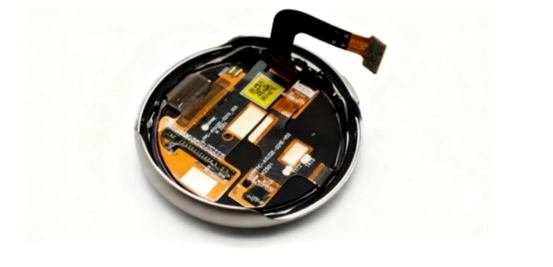
Key point: use the ground layer on the back side as a shielding path. This is commonly adopted in wearable devices such as smartwatches.
Detail 6. How to protect narrow FPCs from stress damage
Narrow FPCs are more vulnerable to stress during assembly, even a bit of pulling or forced bending can cause damage.
Key point
Key point: a typical solution is to add a curved or spring-like section near the active or operation area. This prevents direct force from being transferred to critical regions. 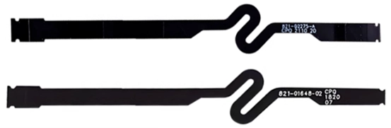
Conclusion
Flexible PCB design requires careful attention to detail to avoid common mistakes that can lead to costly failures. By getting these details right, you can design FPCs that are easy to assemble, provide good shielding, and can withstand harsh electrical and environmental conditions.