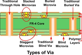
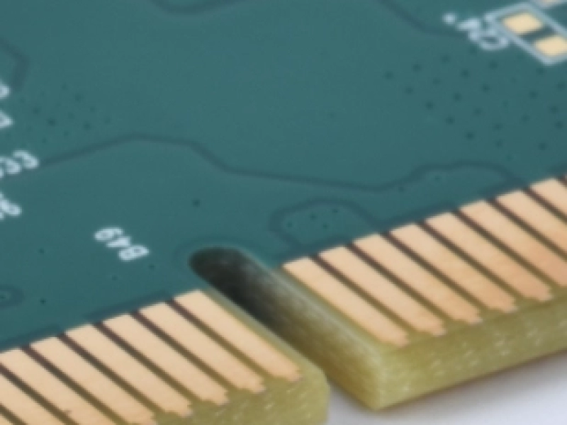
+86(755) 27944155 sales@knownpcb.com
KNOWNPCB

Blog & Design Guide

Blog & Design Guide
Home Blog & Design Guide

HDI Board Introduction

February/03/2026

HDI introduction

High-Density Interconnector (HDI) PCBs are advanced printed circuit boards characterized by a higher wiring density per unit area compared to standard PCBs.  


They incorporate:

  • fine lines
  • microvias,
  • multiple layers

which allow for more compact and efficient designs.

  • Blind / Buried Microvias: Small holes that connect different layers, enabling higher density and reducing the space needed for routing.

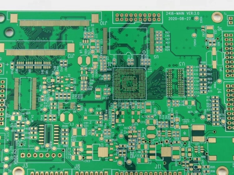
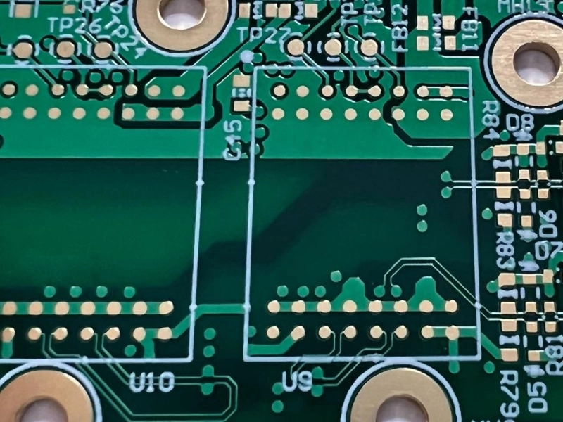
Key Features of HDI PCBs 01


  • stable laser via formation
  • controlled plating and copper filling
  • copper balancing to avoid via fatigue underthermal cycling


  • HDI Board Introduction


  • Smaller trace width and space: HDI PCBs can accommodate smaller components with tighter lead spacing, making them ideal for compact devices.

Key Features of HDI PCBs 02


  • high-Tg FR-4 / FR-5

  • polyimide for wide thermal cycling

  • CTE-matched stackups to reduce warpage


HDI Board Introduction

  • Layer Count: HDI boards often have multiple layers (4 to 20 or more), which support complex circuits and designs.

Key Features of HDI PCBs 03


  • 26 oz copperoptions

  • thermal-via grids
  • heat-spreading planes for MOSFETs / IGBTs /SiC devices

HDI Board Introduction


Impedance Control: Enhanced design capabilities for controlled impedance, crucial for high-frequency applications.

Key Features of HDI PCBs 04


  • bend-radius validation

  • flex-tail stress analysis
  • adhesive-less PI for long bending life

HDI Board Introduction


Applications of HDI PCBs


  • Consumer Electronics: Smartphones, tablets,and wearables benefit from HDI's compactness and functionality.


  • Telecommunications: Ideal for networkingdevices and communication systems.

  • Medical Devices: Essential for compact,reliable medical equipment.

  • Automotive: Used in advanceddriver-assistance systems (ADAS) and infotainment.


Advantages of HDI PCBs   


  • Space Efficiency: Allows for smaller devicefootprints.
  • Performance: Enhanced electricalperformance due to shorter paths and reduced parasitic effects.
  • Versatility: Suitable for variousapplications, from consumer products to industrial systems.     

 More References. 


Submit Your Gerber

Request Stackup Review


Get DFM Review (Free, 24h)


Download our design guides

for better PCB designing and manufacturing

These are some of the design guides designers and engineersdownload the most:

  • DFM Handbook
  • Controlled Impedance Design Guide
  • HDl Design Guide
  • PCB Transmission Line eBook High-Speed PCB Design GuidePCB Material Design Guide
  • DFA Handbook
Check out our design guides

You can submit files via our Message Box for a DFM check and pricing.

Proven by 7 industries, 4000+ customer projects

HDI Board Introduction

Please contact us at sales@knownpcb.com, ask for engineering support here or use the form below to reach out to KnownPCB

Get In Touch Today

Support At:
Upload Gerber/PCB File:
Send Message
Name*
Email*
Company Name*
Address
Job Title
Phone Number