Blog & Design Guide

The function of PCB via protection is a guarantee for solderability, reliability, and long-tern circuit performance. According to IPC-4761, vias are defined as protected through different structures such as tented vias, plugged vias, filled vias, covered vias, and capped vias.PCB designers strategically select the via protection type, balancing the cost, manufacturability, solder mask performance, signal integrity, and reliability requirements in multilayer boards, HDI circuits, automotive electronics, industrial controls, and other demanding PCB applications.
| Vias Holes (According to IPC-4761) | ||
|---|---|---|
Tented Via | A via with a dry film mask material applied bridging over the via wherein no additional materials are in the hole. Single-sided tented is not recommended.  | 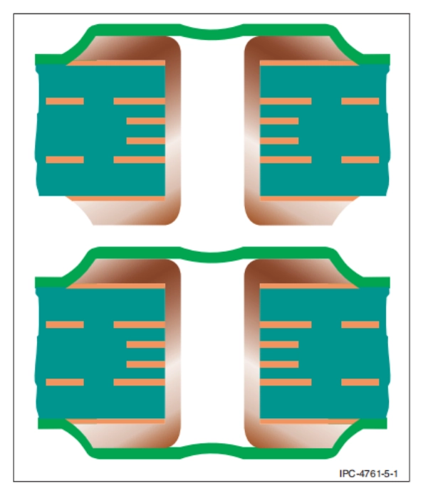 |
Tented and Covered Via | A Type I via with a secondary covering of mask material applied over the tented via. Single-sided tented and covered is not recommended. | 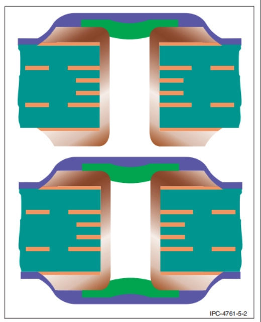 |
Plugged Via | A via with material applied allowing partial penetration into the via. Single-sided plugged is not recommended.  | 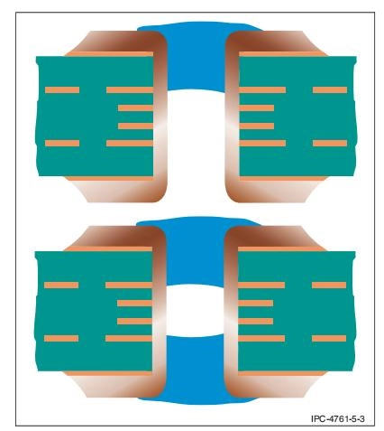 |
Plugged and Covered Via | A Type III via with a secondary covering of material applied over the via. Single-sided plugged and covered is not recommended.  | 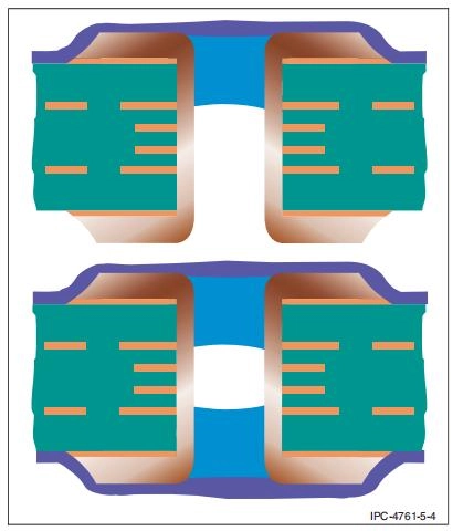 |
Filled Via | A via with material applied into the via targeting full penetration and encapsulation of the hole.  | 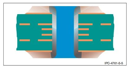 |
Filled and Covered Via | A Type V via with a secondary covering of material (liquid or dry film soldermask) applied over the via. 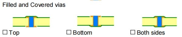 | 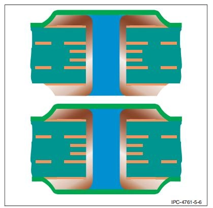 |
Filled and Capped Via | A Type V via with a secondary metallized coating covering the via. The metallization is on both sides. 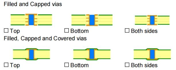 | 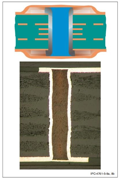 |
Get DFM Review (Free, 24h)
April/16/2026Return-Path Stability as Part of HDI Stackup Design

October/10/2026SMPS PCB Layout: Hot Loops, Return Paths, and EMI Checks
April/16/2026Common Stackup Choices For A Manufacturable HDI Board
March/30/2026The Definition of Through Via, Blind Via, Buried Via

October/09/2026Single-Sided PCB Routing: Jumpers, Return Paths, and Width
 | Download our design guidesfor better PCB designing and manufacturing These are some of the design guides designers and engineersdownload the most:
|
Proven by 7 industries, 4000+ customer projects
Please contact us at sales@knownpcb.com, ask for engineering support here or use the form below to reach out to KnownPCB | Get In Touch Today |