Get A Quote
CN

PCB warpage is a common issue in both manufacturing and assembly. A board that looks slightly bent may already cause serious problems in SMT. As electronics move toward higher precision and smaller components, flatness becomes more critical than ever.
This article explains what PCB warpage is, why it happens, and how to control it during design, fabrication, and assembly.
PCB warpage refers to the bending or twisting of a printed circuit board that was originally flat.
There are two main types:
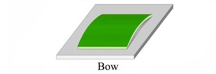
Bow means the board curves along its length or width. The center lifts up while the edges touch the surface.
Calculation formula:
Bow = (Maximum height at center / PCB length) × 100%
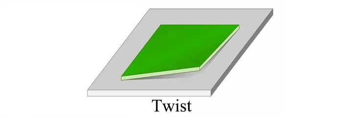
Twist happens when one corner lifts while the other three corners stay flat. The board deforms along the diagonal.
Calculation formula:
Twist = (Corner height / Diagonal length) × 100%
PCB warpage affects both manufacturing and reliability.
According to industry requirements such as IPC-6012, typical flatness limits are:
≤ 0.75% for SMT boards
≤ 1.5% for non-SMT boards
In high-precision assembly, some factories require ≤ 0.5% or even ≤ 0.3%.
Warpage can cause:
Poor component placement accuracy
Solder joint defects
BGA open circuits
Difficulty during depaneling
Assembly interference with chassis or connectors
As noted in the uploaded material, uneven boards can even damage automated insertion machines . In SMT lines, positioning errors and soldering problems are common results .
In short: even small deformation can create big problems.
PCB warpage is usually caused by internal stress imbalance. It can come from design, materials, fabrication, or assembly.
PCB is made of copper foil, resin, and glass fiber. Each material has a different coefficient of thermal expansion (CTE).
For example:
Copper CTE ≈ 17 × 10⁻⁶
FR-4 Z-axis CTE below Tg ≈ 50–70 × 10⁻⁶
Above Tg, FR-4 expands much more
When heated and cooled, these materials expand and shrink at different rates. This creates internal stress.
If the Tg (glass transition temperature) is low, the board softens during reflow (above 240°C). Permanent deformation may occur.
If prepreg (PP) layers are not symmetrically arranged, stress distribution becomes uneven. This is a common reason for multilayer PCB warpage.
If one side has large copper planes (GND or power), and the other side has sparse traces, thermal shrinkage becomes uneven.
After etching, stress is released differently on each side. The board bends toward the side with less copper.
Adding thieving copper (balanced dummy copper) can reduce this effect.
Lamination is one of the biggest sources of thermal stress.
If temperature, pressure, or cooling rates are not well controlled, resin curing becomes uneven. Internal stress remains trapped inside the board. Later processes such as drilling or routing may release this stress and cause warpage.
Uneven solder mask thickness
Uneven curing
HASL (Hot Air Solder Leveling) thermal shock
During HASL, the board enters molten solder at around 250°C and then cools rapidly. Sudden heat and cooling can cause bending.
Improper storage (vertical leaning or stacking)
V-CUT depaneling damage
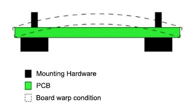
Heavy components on large boards
Uneven screw tightening
Mechanical force can distort thin boards, especially those under 2.0 mm thick.
Reflow is a major stress event.
The board heats from room temperature to over 240°C and then cools down again. If internal stress already exists, reflow can permanently deform the PC.
The best solution is prevention during design.
Keep prepreg and core layers symmetrical
Balance layer thickness
Use the same supplier materials
Add dummy copper in sparse areas
Keep top and bottom copper area similar
Design power and ground layers symmetrically
For lead-free assembly, use Tg ≥ 170°C materials. Higher Tg improves dimensional stability .
Avoid heavy components near V-CUT lines
Reduce board size when possible
Avoid very thin large panels
Pre-baking at 120–150°C removes moisture and releases internal stress .
Follow correct temperature profile
Avoid rapid cooling
Ensure even pressure distribution
Bake multilayer boards at 150°C for several hours to reduce internal stress .
Allow natural cooling on a flat surface instead of rapid water cooling .
Store boards flat on stable racks. Avoid vertical leaning.
If boards are stored long-term, bake them before assembly to remove moisture .
Avoid excessive peak temperature
Use smooth heating and cooling curves
For thin or large boards, use high-temperature carrier fixtures to support the board.
Use routing instead of aggressive V-CUT
Avoid manual bending separation
Measurement method:
Place the PCB freely on a flat surface. Measure the maximum height difference.
Formula:
Warpage (%) = (Height / Board length or diagonal) × 100%
Typical industry limits follow IPC-A-600:
SMT boards: ≤ 0.75%
Non-SMT boards: ≤ 1.5%
Some high-end applications require ≤ 0.5%.
PCB warpage is not caused by one single factor. It is the result of:
Material mismatch
Stack-up imbalance
Uneven copper distribution
Thermal shock
Mechanical stress
The most effective solution is prevention in the design stage. Symmetrical stack-up, balanced copper, and high Tg materials reduce risk from the beginning.
Then, strict process control during fabrication and assembly ensures stable performance.
Warpage control requires cooperation between PCB designers, manufacturers, and assembly factories. When managed properly, it can be reduced to a very low and controllable level.
Request for a tech support
 |
Download our design guidesfor better PCB designing and manufacturing These are some of the design guides designers and engineersdownload the most:
|
Proven by 7 industries, 4000+ customer projects
|
Please contact us at sales@knownpcb.com, ask for engineering support here or use the form below to reach out to KnownPCB |
Get In Touch Today |