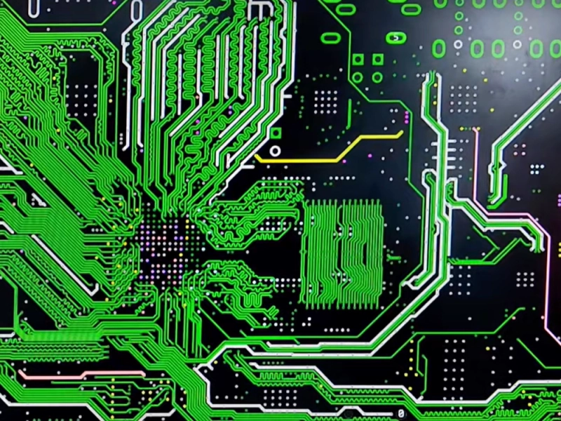
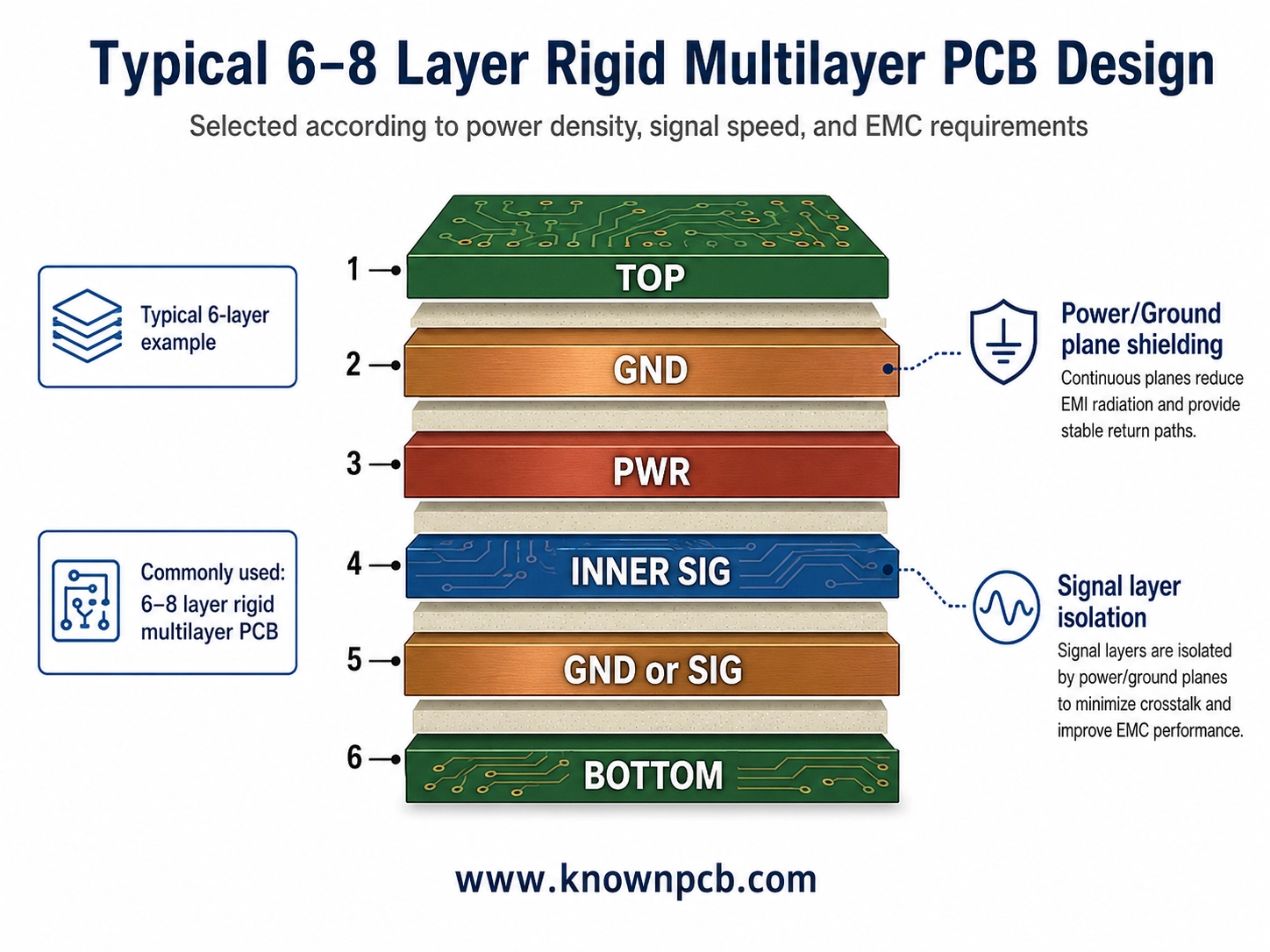
The stackup with a 6-to-8 layer is a typical PCB design for multilayer PCB subject to power densities, signal integrity, and EMC.
It is optimal to adopt a structure with 8-layer design for higher power density or high-speed interfaces in PLC, as it accommodates additional dedicated reference planes and split power layers.
Low-loss PCB material, such as Panasonic Megtron 6、Isola I-Tera MT40, perform excellently in minimizing dielectric loss and ensuring impedance consistency for industrial motor control equipment requiring high-speed or high-integrity signals.
High Tg FR-4, exemplified by Isola 370HR , is recommended to be used in PLC with moderate signal speeds. With respect to maximize ampacity and thermal spreading, KnownPCB suggests incorporating thick-copper cladding, thermal pillars, and metal-base PCBs are effective for boosting current-handling capacity and dissipating heat from concentrated sources.
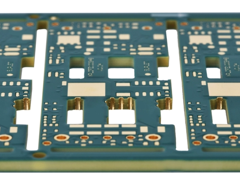
Power Loops: The IGBT/MOSFET main power loop follows the “short, wide, low-inductance” rule. A recommendation of copper weight is ≥2oz for high-current paths, it is reinforced with parallel copper pours, busbars, via arrays, or embedded copper structures. Vias are sized based on amperage, plating specs, and thermal limits to ensure reliability.
Safety Isolation for PLC: The recommendation of minimum distance is 8mm for both clearance and creepage for High-voltage (HV) and low-voltage (LV) control domains within PLC PCB with systems operating at 600V or above. Additionally, galvanic isolation can be achieved via isolation barriers, including slotted routing, opto-isolators, or isolated power modules. Crucially, it is mandatory to calculate the distance according to pollution degree, CTI, and operating altitude to prevent dielectric breakdown.
Signal Integrity, SI for PLC: Differencial signals for PCB layout in PLC, such as those for encoders and communication buses, undergo strict impedance control (at 100Ω ±10%) to prevent reflections, while match lengths within 5mm. Furthermore, the layout prioritizes distance from noisy switching nodes for sensitive analog paths. PLC PCB layout designers leverage RC filtering and shielding traces when a dedicated 20mm separation is unachievable. To this end, Kelvin sensing and solid ground references are essential to mitigate the impact of high dv/dt interference.
Thermal Management: Power component footprints or thermal spreading area is designed with extensive copper pours, thermal via arrays, or embedded copper slugs. Meanwhile, it is verified through rigorous thermal simulations and prototype temperature-rise testing. The junction temperature (Tj) is targeted typically a threshold below 125°C, which as a generous safety buffer remains within the limits specified in the datasheet.
Work with KnownPCB for multilayer PLC PCB stackup design, low-loss PCB material selection, high-current copper design, safety isolation, signal integrity, and thermal management.
Get a PLC PCB Quote | Download our design guidesfor better PCB designing and manufacturing These are some of the design guides designers and engineersdownload the most:
|
Proven by 7 industries, 4000+ customer projects
Please contact us at sales@knownpcb.com, ask for engineering support here or use the form below to reach out to KnownPCB | Get In Touch Today |