The edge connectors possesses excellent electrical conductivity, ensuring efficient signal and current transmission.
Additionally, it offers strong corrosion resistance, effectively withstanding oxidation and corrosion.
Lastly, gold fingers exhibit robust mechanical strength, capable of enduring repeated insertion, removal, and contact pressure.
| Type | Description |
|---|---|
| General Gold Finger | Horizontal or evenly aligned fingers with uniform length and width. |
| Long-and-Short Gold Finger | Finger pads share the same width but differ in length. |
| Segmented Gold Finger | Segmented fingers with varying lengths and non-continuous layout. |
 |  |
| Category | Description |
|---|---|
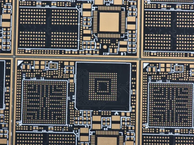
| Characteristics | Gold fingers provide excellent conductivity, corrosion resistance, and mechanical durability,supporting stable signal transmission and repeated mechanical contact. |
| Function | They serve as reliable electrical contact interfaces between PCBs and connectors or card slots. |
| Application Fields | Widely used in mobile phones (SIM and battery connectors), computers (memory and expansion card slots),and automotive electronics such as dashboards, infotainment, and navigation systems. |
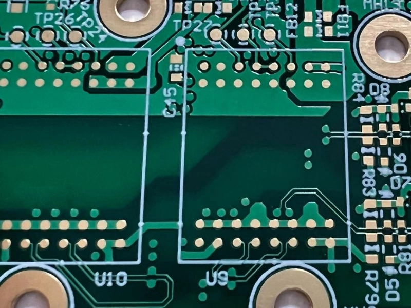
PCB designers typically stick to the standard 1.0, 1.27, or 2.54mm for picth and pinout. The main idea here is to maintain compatibility with those off-the-shelf components.
PCB designers got to prioritize differential impedance matching when evaluate signal integrity—the usual 90 or 100Omega for PCIe and USB, just to stay ahead of any EMI or data loss issues.
Robustness:
Evaluate mating cycle ratings based on the product’s expected use case; integrate staggered pin lengths if hot-swapping is a priority.
One more thing on form factor—
Define critical tolerances for PCB thickness and edge beveling to guarantee a secure and reliable fit within the connector housing.Get DFM Review (Free, 24h)
 | Download our design guidesfor better PCB designing and manufacturing These are some of the design guides designers and engineersdownload the most:
|
Proven by 7 industries, 4000+ customer projects
Please contact us at sales@knownpcb.com, ask for engineering support here or use the form below to reach out to KnownPCB | Get In Touch Today |