Summary: This article provides a comprehensive overview of HDI printed circuit boards manufacturing technology, common issues and their solutions, material selection, and quality control systems, while also covering application advantages and frequently asked questions.
1. Intro
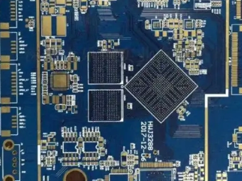
HDI printed circuit boards achieve high-density routing by assembly technologies such as BGA and CSP. It meets the demands for high-speed, high-frequency transmission and compact size.
2. Frequently Challenges and Solution During Our HDI Printed Circuit Boards Manufacturing
HDI printed circuit boards are widely applied in high-performance devices. And we have done lots of research on the challenges and solutions of PCB HDI printed circuit boards manufacturing market.
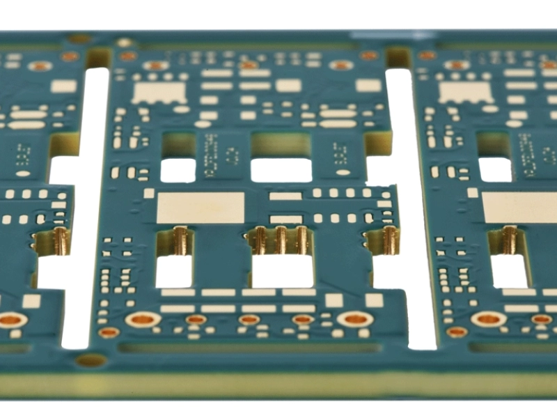
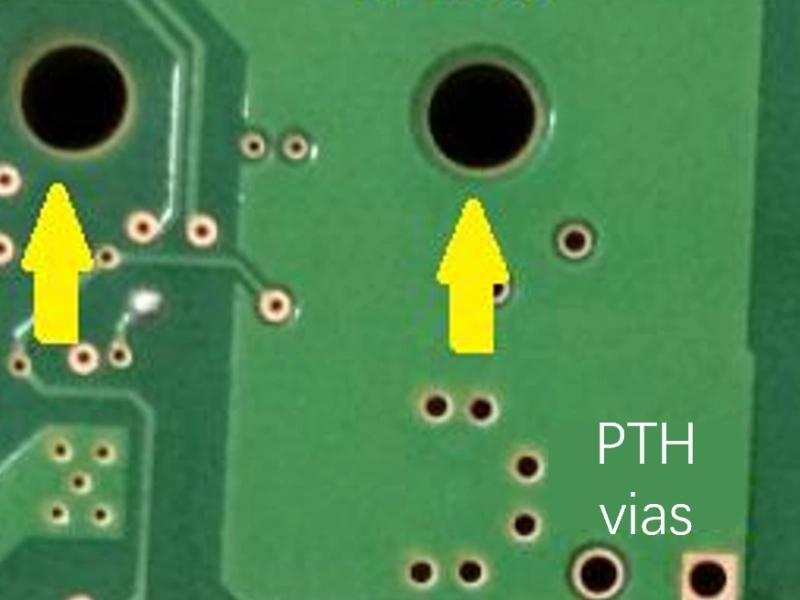
- Uniform Hole Diameter
The hole diameter may exhibit non-uniformity during laser drilling and mechanical drilling processes. This challenge can result in the circuit board failure to meet design specifications.
Solution: We recommend using high-precision laser drilling technology and ensuring the stability of the drilling equipment. Meanwhile, we can optimize the size and placement of holes during the design phase to minimize unnecessary variations in hole diameter.
- Poor Inter-layer Connection
During the manufacturing of HDI printed circuit boards, defects in inter-layer connections may lead to signal transmission failure or circuit disconnection.
Solution: Advanced plating technologies can improve the quality of inter-layer connections and strengthen quality control during the plating process. High-quality substrate materials and reliable packaging techniques can also effectively prevent issues with inter-layer connections.
- Uneven Thermal Expansion
Thermal expansion of PCB materials in thermal cycling process can cause board deformation and bad circuit stability.
Solution: It would be better to select appropriate PCB substrate materials, like those with good thermal stability. Another way is to optimize thermal management designs.
3. Advanced Manufacturing Technologies
3.1 High-precision Laser Drilling Technology
UV laser drilling technology with 355 nm wavelength can produce micro-blind vias, which can be typically between 75 and 150 μm in diameter. The non-contact process eliminates copper foil displacement, while traditional drilling cause mechanical stress. So the quality can be ensured by smooth via walls.
3.2 Advanced Plating Technologies
Pulse plating manufacturing technology enhances the continuity and adhension of the copper layer. The regulating forward and reverse currents can optimize the ion distribution within high-aspect-ratio microvias (≥5:1). So the dog-bone effect and void formation are suppressed. According to our record, the fill rate can exceed 98%.
3.3 Build-up Method and Multi-stage Lamination
This manufacturing technologies perfectly suit the complex packages in which BGA pin pitches are less than 0.35mm. Build-up and multi-stage lamination includes the sequential application of resin coated copper, vacuum hot pressing, and laser drilling to achieve high density interconnection.
3.4 Modified Semi-Additive Technologies
It is mainly applied to ultra-fine circuitry which line widths and spacings is less than 30 μm, such as in 224Gbps high-speed PCB. The process can produce copper lines with vertical cross-sections by seed layer deposition and selective plating. Compared to traditional subtractive methods, it significantly reduces the undercutting issues.
4. Materials Selection for HDI Printed Circuit Boards
A good HDI printed circuit boards manufacturing also root in material selection. For example, Special FR-4 and modified epoxy substrate contributing to more even thermal expansion. In particular, it is recommendable to use modified epoxy substrates which Tg is higher than 170°C and Z-axis CTE is lower than 50 ppm/°C. This enhances the thermal shock resistance of multilayer boards.
In addition, there are other tips about materials selection for HDI printed circuit boards.
PCB Type | Recommended Material (Parameter/Board Type) |
5G and millimeter-wave PCB | Dk ≤ 3.5 , Df ≤ 0.005 (e.g., Rogers, Shengyi S1000-2M, or PTFE-based substrates) |
Standard HDI PCB | Tg ≥ 170°C FR-4 |
Automotive or industrial control PCB | High-Tg or low-CTE FR-4 or BT resin |
RF/high-speed digital PCB | Low Df Composite materials (e.g., hybrid laminates) |
5.Quality Assurance of HDI Printed Circuit Boards Manufacturing
There are two universal quality risks for HDI printed circuit boards manufacturing as our produce experience. How to manage the quality risk is very important.
- The first common one is micro-via overhang, undercut, and via-fill voids. It is caused by uncontrolled laser drilling parameters or uneven post-drilling brown oxide treatment. This quality risk can be solved by UV or CO₂ hybrid laser technique. For many cases, we control Ra ≤ 2μm and use vacuum pulse plating to achieve void-free filling. Last but not least, X-Ray testing is very useful to detect the problems. The board is put into the chamber depth of the testing machine. This is the reason why you can not see it in the photo haha. And the X-Ray can go through layers of the PCB and check every via clearly as what the machine screen shows.

- l Interlayer misalignment and delamination. Generally speaking, it is caused by uneven prepreg resin flow and moisture absorption in the base material. Using low-flow PP and choosing base material, which Tg is less than 145°C, can perfectly improve the quality. And we often inspect voids by post-lamination C-SAM Technology.

On a macro level, we are also certified by ISO9001. Besides the above X-ray and C-SAM quality testing machine, we have others like automatic optical inspection machines. The whole product line is well equipped by multiple quality assurance nodes.
During the incoming quality control stage, we KnownPCB apply 2D measuring systems and microscopes. Key inspections focus on the dimensions and warpage of the substrate as well as oxidation or scratches on the copper foil. After etching the inner-layer circuitry, inspecting the quality of the traces themselves is critical. We typically employ automated optical inspection equipment. AOI allows for the rapid detection of circuit defects such as open circuits, short circuits, nicks, pinholes, and residual copper.
Following the lamination and drilling stages, we inspect the multi-layer boards for inner-layer hole registration accuracy and hole-wall roughness by X-ray drilling machines. For HDI boards, we sometimes use automated X-ray inspection to check for inner-layer misalignment. A second AOI inspection is subsequently executed after the outer-layer circuitry has been etched.
After the solder mask exposure and development processes, a third AOI inspection or high-magnification microscopes would be conducted. They mainly check for detached solder mask bridges, ink encroachment onto pads, and the presence of air bubbles or foreign matter beneath the solder mask.
For final product testing, we use flying probe testers to verify electrical performance, ensuring that every circuit path is continuous and free from interference. If required by the customer, impedance testers can also be used to verify that the characteristic impedance meets specifications.
6. The Advantages of HDI Printed Circuit Boards
The core advantages of HDI printed circuit boards lie in higher integration. If the final product is a smart phone or wearable device, HDI printed circuit boards can be very helpful. It is very lightweight and more compact.
The second advantage is superior electrical performance. The signal paths in HDI printed circuit board are shorter than the others. And the shorter signal path can greatly reduce parasitic inductance and capacitance, so the signal transmission quality for high-speed would be better. Besides, micro-via structures of HDI printed circuit board can improve impedance control and effectively suppress interference of RFI, EMI ESD.
It is very suitable for high-end portable, high-speed, and high-frequency electronic devices.
7. How To Take HDI Printed Circuit Boards from Design to Manufacturing
The entire process needs no inventory stocking and no purchase of SMT Steel Stencil. We provide a turnkey service that covers online file upload, internal factory design review and quoting, transparent production, and shipping.
FAQ
1. What Is a HDI PCB Board?
HDI printed circuit boards is an advanced PCB that achieves ultra-high wiring density by micro-blind vias, laser drilling, and fine-line technology. Its core features include line width/spacing ≤100μm and microvia diameter ≤150μm (typically 50–127μm). And blind vias, buried vias, or any-layer interconnect structures can be made in HDI PCB Board.
2. Are Printed Circuit Boards Worth Anything?
Brand-new/unused PCBs have a market value, depending on the model, layer count, and material. Unit prices for standard single- or double-sided boards range from a few dollars to several hundred dollars.
3. How Much Gold Is in a Pound of Circuit Boards?
One pound (approximately 0.454 kg) of scrap circuit boards typically contains between 0.018 and 0.34 grams (i.e., 18–340 milligrams) of gold, depending on the type and source of the board. Specifically, common computer or mobile phone motherboards contain approximately 0.05–0.15 grams per pound.
References
Johnson, H. W., & Graham, M. (2003). High-speed signal propagation: Advanced black magic. Prentice Hall.
Howard Johnson, M., & Graham, M. (2020). High-speed digital design: A handbook of black magic (2nd ed.). Prentice Hall.
Ott, H. W. (2011). Electromagnetic compatibility engineering. John Wiley & Sons.