Summary: This article provides a clear comparision between PCB Vs PCBA. It includes their definitions, applications, costs and relations in manufacturing. Also, the differences between PCB Vs motherboard are mentioned.
1. Intro about PCB Vs PCBA
PCB means printed circuit board, while PCBA is about assembly. The former is the bare board only without electronic components attached, the latter is fully assembled PCB with components soldered onto it.
2. What Is PCB?
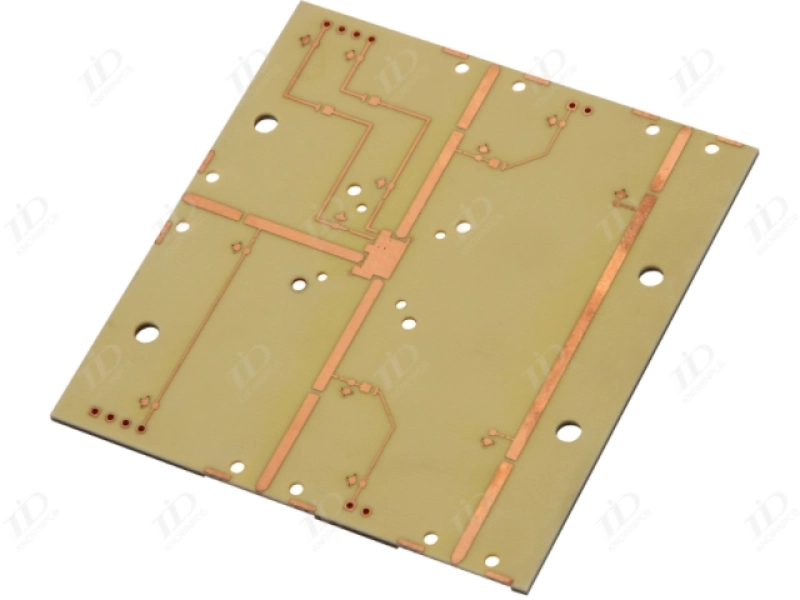
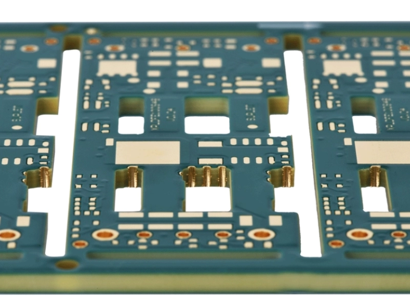
Let’s start from introducing PCB first. PCB is a board that overlaid with conductive copper foil traces for electronic components connection. Its substrate is an insulating board, which is commonly made of materials such as fiberglass or epoxy resin.
If you ask me the application of PCB, it has no functionality on its own because no components have yet been soldered onto it. It serves as an intermediate product between raw materials and final products. It is very applicable for R&D prototype validation or small-batch final product DIY. You can try different component assembling on the bare PCB till finding the optimal solution.
3. What Is PCBA?
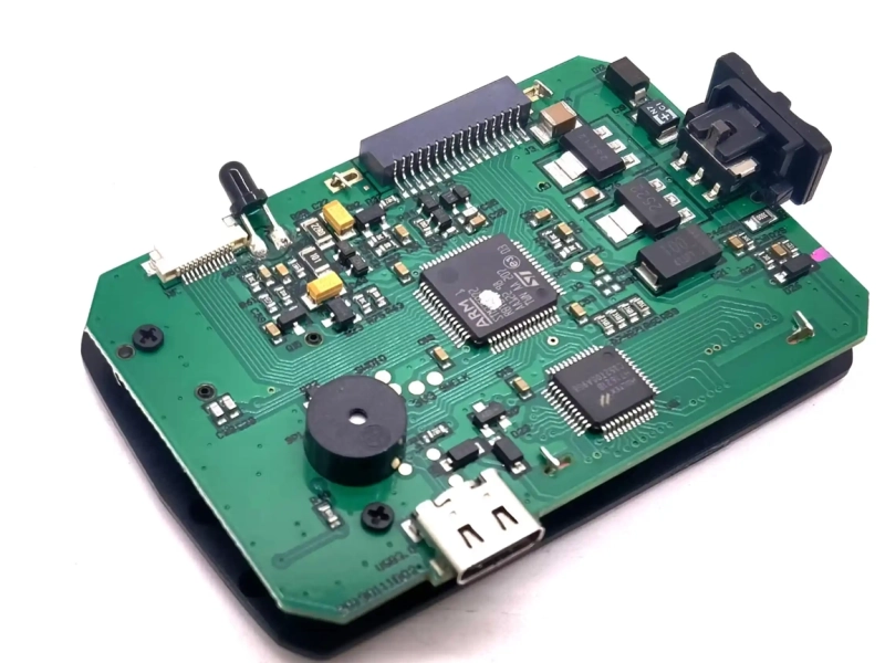
And PCBA refers to the process of mounting and soldering all necessary components onto a bare PCB, like resistors, capacitors, and chips. Then it becomes a part with comprehensive electrical functionality.
For its advantages, it is a functional unit that can be directly installed into a product and powered up for operation. It can apply in the final product in the field of consumer electronics, automotive electronics, industrial control, medical equipment, communication equipment and smart home.
4. What Are the Main Differences Between PCB Vs PCBA?
To sum up, a PCB is a bare circuit board without soldered components, whereas a PCBA is a PCB that has undergone the mounting and soldering of all components. If you need a functional finished product, choose a PCBA. Engineers who want to verify a circuit design can only buy PCB.
5. How Do PCBA and PCB Relate to Each Other?
They are related to the manufacturing process. The PCB manufacturing process is followed by PCBA. They both constitute the core manufacturing chain for electronic products.
5.1 PCB Manufacturing Process Is the Preceding Step.
In the PCB manufacturing process, it starts from material cutting, which is also called panel cutting. The large sheets of copper-clad laminate, which is the fiberglass-reinforced epoxy resin clad substrate, are cut into the working panel sizes. Then, the product line would conduct edge treatment and deburring to prepare the panels for subsequent processing.Later, if final product is multiple layer, inner layer circuit production counts a lot. The product line workers and machine apply photosensitive dry film onto the copper-clad board surface, which the substrate is inside. Then, pattern exposure step would follow the above step. That is, the circuit pattern can move onto dry film by direct laser imaging technology. The unexposed part of dry film will disappear and only the required copper still stays on.
Next, chemical etchants will etch the copper which no dry film protects. Only the substrate will then expose. Finally, the reserved dry layer will be eliminated. Only the inter-layer copper circuit stays there. In common, professional factories will apply AOI testing after the inner-layer circuit board manufacturing step.

If you can easily understand the inter-layer manufacturing step, the following processes would be simple. After finishing brown-oxide treatment to inter-layer circuits, the product line will stack it with prepreg and copper foil. Then this stack becomes a single unit under high temperature and high pressure.
Next, the CNC machine will drill all holes on the board and ensure no remaining resin debris.
The hole walls will then undergo chemical copper deposition to establish metal interlayer electrical connectivity.
Outer-layer circuitry process is similar as inter-layer’s. It includes film lamination, exposure, and development, exposed circuit areas thickening, tin layer covering and subsequent etching. After etching, the precise circuit still has to receive AOI testing to ensure quality.
Solder mask will then be applied. The next process, exposure, can show and leave the pads. The following thermal curing can provide insulation and solder protection. The remaining pads then undergo surface finishing (such as HASL, ENIG, or OSP) to prevent oxidation and enhance solderability.
Then, the screen printing process will print the logo and component location marks, which the low-temperature baking machine will fix and dry. Now the board is almost finished, but they still connect together in a whole panel. CNC milling machine will cut the panel into individual units and fix the edge into V-grooves shape for easy depaneling.
The electrical testing checks can only detect short circuits and open circuits, while final inspections cover appearance, dimensions, and reliability sampling. Finally, the product line workers will clean, dry, vacuum-packed the PCB with desiccant and labeled. This is the whole manufacturing process of PCB.
5.2 PCBA Process Is the Following Step.
PCBA process closely follow the PCB manufacturing process. The factory first prepares all electronic components based on the bill of materials. Production line operators load bare PCBs onto an automated conveyor track. A fully automatic solder paste printer precisely deposits solder paste onto the PCB pads. The paste can temporarily hold components in place and provide conductive connections.
Next, a high-speed pick-and-place machine uses vacuum nozzles to pick up miniature components and rapidly mount them onto the solder paste according to programmed coordinates. Sometimes, not all the components are small. So multi-function placement machine will handle the precise mounting of large or irregularly shaped components.
After that, the assembled circuit boards then enter a reflow oven, where multiple heating zones gradually raise the temperature. It will melt the solder paste to form permanent solder joints. Then, a cooling zone can solidify the joints, completing the surface mount process.
Let’s move on to the wave soldering process. Automated insertion machines place through-hole components into the corresponding holes on the finished PCB. And then the next wave soldering machine generates a flowing wave of molten solder beneath the board. It solders the leads of all through-hole components, ensuring electrical connectivity.
Finally, the product line will clean equipment removes flux residues from the board surface. A packaging machine places the qualified PCBAs into anti-static bags.
6. How to Choose PCB VS. PCBA
You should choose a PCB when you require only the bare circuit board substrate. For instance, you may want to verify a circuit design during the R&D phase. Or you would like to source components yourself for subsequent assembly.
When you need a complete functional board with all components already welded, you should choose PCBA. Sometimes, your product is in mass production, but there is no expensive surface mount equipment for manufacturing.
7. Both of Our PCB and PCBA Services
If you want both PCB and PCBA services, we Knownpcb are pleased to provide them. For example, some of our customers first procure a small batch of PCBs to test circuit reliability, and only after verification do they commission the PCBA process to produce the finished product.
Frequently Asked Question
1. What Is the Cost of PCBA Vs. PCB?
For the same 4-layer board, only PCB might cost 0.74 to 1.48 USD per unit in high-volume production. If adding all the components and SMT process, the PCBA price can rise to 7.38–29.53 USD per unit. And it depends on component density and type.
2. What Are the Differences Between PCB Vs. Motherboard?
A motherboard is one of the specific PCB types. While PCB refers to all printed circuit boards, motherboard specifically means the main board in a computer. It connects core components, such as the CPU and memory.
3. What Are the Differences Between PCB Vs. Breadboard?
PCBs are permanent, whereas breadboards are temporary. A PCB is a fixed circuit board manufactured through processes such as etching and drilling, with circuits permanently connected via copper foil. So it is suitable for mass production and long-term application. A breadboard is a reusable prototyping tool, which features a surface filled with spring-loaded sockets. It allows users to freely insert components and build circuits without soldering. So it is ideal for rapid verification, teaching, and debugging.
References
Coombs, C. F., & Holden, H. T. (Eds.). (2016). Printed circuits handbook (7th ed.). McGraw-Hill Education.
Garzon, F. H. (2008). Printed circuit assembly design. Newnes.
IPC. (2023). IPC-A-610: Acceptability of electronic assemblies (Rev. H). IPC.