Summary:
The power supply PCB board is designed to handle electrical energy. This article will mention some useful tips about power supply PCB board design with some purchasing guides.
1. What Is Power Supply PCB Board?
The power supply PCB board is designed to handle electrical energy. It is the core physical carrier of the power system, such as switching power supplies and power adapters. It is responsible for converting electrical energy into stable power that can be used. Later, it will efficiently distribute the converted electrical energy to each functional module of the device.
Besides, a good power supply PCB board can ensure that the output voltage and current remain stable under various loads and input conditions. It can also have protection functions. For instance, it can integrate circuits such as over-voltage protection, over-current protection, short circuit protection, and over-temperature protection. This ensures the safety of the power supply itself and the safety of its connecting devices.
2. Types of Power Supply PCB Board
If we classify the power supply PCB board by the most common used method, there can be three types.
Single-sided Type
Only one conductive copper foil layer cover on the substrate side. All circuits and components stay on that side. This type of power supply PCB board structure is the simplest one with the lowest cost. And the design and manufacturing are the easiest. Most of our customers apply single-sided panel low-cost consumer electronic products, such as toys, calculators, simple power supplies, and some lighting fixtures.
Double-sided Type
Conductive copper foil layers cover both sides of the substrate. And the metallized holes allow good connection between both sides. It has larger wiring space for more flexible design. And it can contain more complex circuits with high cost-effectiveness. It suits lots of electronic products, such as household appliances, computer peripherals, industrial control boards, instruments and meters.
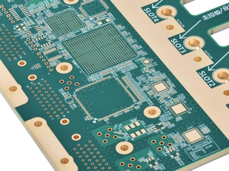
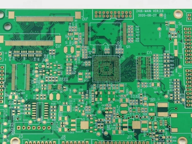
Multi-layer Type
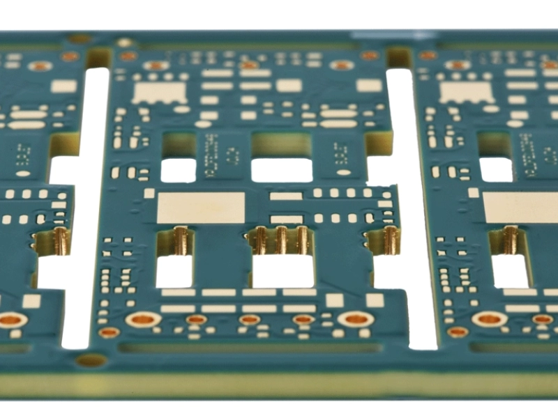
Alternating layers of conductive copper foil and insulating substrate through compression. The layers are connected through metallized holes. Common multi-layer type can be 4-layer boards, 6-layer boards, and 8-layer boards. Features: Extremely high wiring density, strong anti-interference ability, capable of achieving good impedance control, excellent electromagnetic compatibility, complex design, high cost, and complex manufacturing process.
Applications: Complex, high-performance, and high-density electronic products, such as computer motherboards, server motherboards, smartphone motherboards, graphics cards, communication equipment, high-end medical equipment, aerospace electronic equipment, etc.
3. Power Supply PCB Board Design Tips

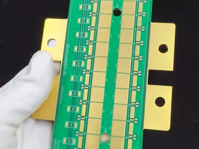
When designing the power supply PCB boards, it is essential to consider their ability to handle high currents. KnownPCB highly recommend to make the traces wider and increase the copper thickness, or even use copper-filled areas. This can reduce resistance, lower voltage, temperature rise, significantly reducing the risk of overheating and damage. As for the copper foil weight, power supply PCB boards typically use heavier copper foil, such as 2oz, 3oz or higher. Additionally, electronic designers usually design multiple, large-diameter vias or filled vias to enhance the current-carrying capacity of the large current path.
Secondly, the designer should ensure that the high-voltage and low-voltage parts are properly separated according to strict safety standards, such as those specified by UL and IEC. Sufficient creepage distance and electrical clearance can be helpful. This will effectively reduce the risk of high-voltage breakdown. The recommended approach is to use clear isolation barriers, such as grooves, and use optocouplers for electrical isolation.
The heat dissipation design is a crucial aspect. First of all, we need to identify which components are heat-generating elements. They can be semiconductors, transformers, inductors, and resistors. And properly arranging these heat-generating elements can help with better heat dissipation. As for the cooling measures, we have several recommended common methods.
- A large area of bare copper sheet serves as a heat sink
- Using heat dissipation pads
- Adding heat sink mounting holes or directly designing heat sink mounting positions
- Connecting to the metal shell
- Sometimes, additional heat sinks are required
For some cases, we also suggest minimizing the critical loop, especially for the path of the power switch circuit. It includes input capacitor, switch transistor, transformer, inductor, output capacitor. All these circuits should be as short and wide as possible to reduce parasitic inductance and electromagnetic interference.
And if what you are handling is sensitive control signals PCB, we advise you to do the signal and power separation. For example, feedback and PWM signals circuit part should be routed away from the power lines that have high noise. In necessary cases, using ground lines and designing multi-layer boards can shield the noise, too.
Last but not least, don’t forget to consider a good grounding strategy. For power supply PCB board, we recommend star-shape grounding, single-point grounding or ground plane separation. Then, setting a clear grounding point can reduce ground loop noise.
4. How to Choose Power Supply PCB Board OEM Services?
When we choose the power supply PCB board OEM service, we can focus on multiple aspects including high current carrying capacity, stability of heat dissipation technology, and compliance with safety regulations. Compared to ordinary consumer electronics, the power board needs better thick copper, better impedance control, and better insulation spacing.
4.1 Manufacturing Technique and Material Handling
A good manufacturer can process 2oz-10oz thick copper plates. If they can handle side etching issues under high current conditions, that should be better. Besides, we can also double check their compliance with UL/IEC standards. Some manufacturers can offer proper substrate selection based on power density and control of dielectric constant and loss factor to optimize signal integrity. That is very recommendable.
4. 2 Compliance with Qualifications and Quality System
The common industry certification threshold is ISO9001 basic certification for quality assurance. For automotive or industrial scenarios, we can also ask the potential manufacturing to show IATF 16949 automotive-grade certification. For international export products, it is necessary to confirm the validity of UL, RoHS, and REACH certifications.
FAQ
1. What Is the Power Supply in a PCB?
Power supply does not refer to a single component, but rather a complete power supply system. It provides stable and appropriate voltage and current for all the electronic components on the board. It includes the entire chain from the external electrical energy input to the final distribution to the chips.
2. Can a PCB Handle 12V?
Yes, the PCB is fully capable of handling 12V voltage. This is a very common low-voltage level in electronic design. The withstand voltage of standard FR-4 board materials is far higher than this value.
3. Do PCB Use DC or AC?
The electronic components on the PCB mainly work under direct current (DC), while their input power supply may be alternating current (AC).
References
- Chen, J. Z., Pang, Y. F., Boroyevich, D., Scott, E. P., & Thole, K. A. (2002). Electrical and thermal layout design considerations for integrated power electronics modules. Conference Record of the IEEE Industry Applications Society Annual Meeting, 1, 242–246. https://doi.org/10.1109/IAS.2002.1044115
- Musznicki, P., Schanen, J.-L., Allard, B., & Chrzan, P. J. (2004). Accurate modeling of layout parasitic to forecast EMI emitted from a DC-DC converter. In Proceedings of the 35th IEEE Power Electronics Specialists Conference (PESC) (Vol. 1, pp. 278–283). IEEE. https://doi.org/10.1109/PESC.2004.1355756
- Wang, S., Lee, F. C., Chen, D. Y., & Odendaal, W. G. (2004). Effects of parasitic parameters on EMI filter performance. IEEE Transactions on Power Electronics, 19(3), 869–877. https://doi.org/10.1109/TPEL.2004.826527