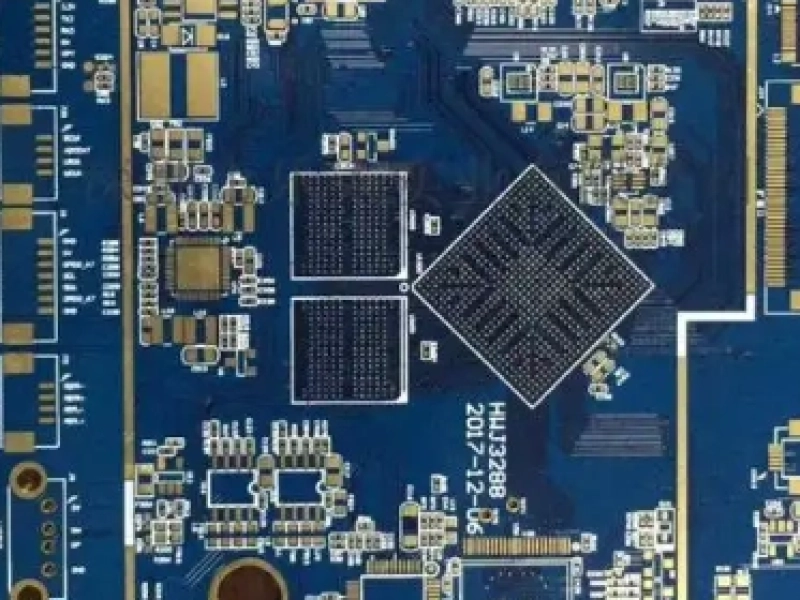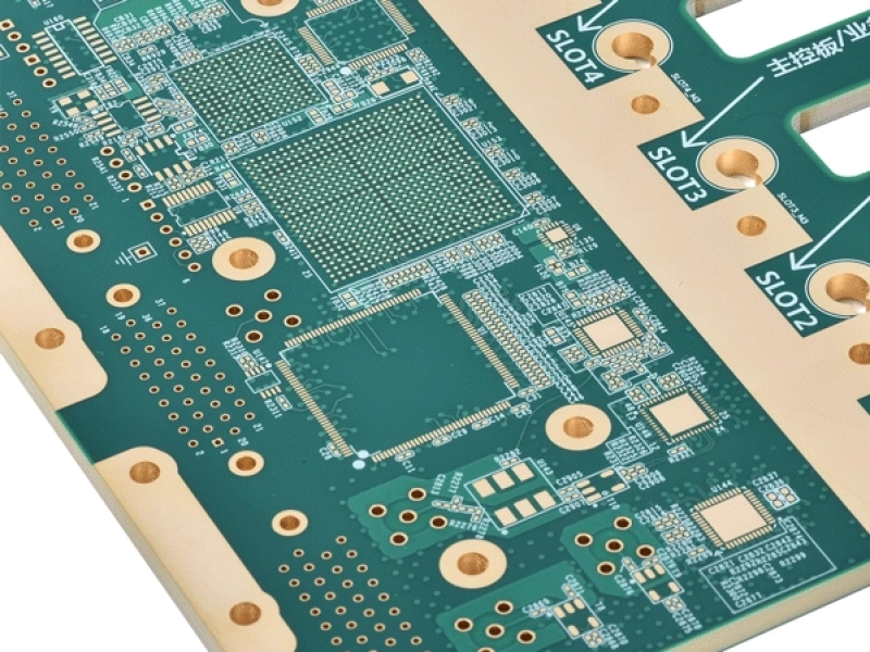
In high-reliable and manufacturable HDI design, we often regard stackup of a HDI board as a layer arrgangement. However, in the real practice, the function of the HDI board structure is not just about the layer of HDI PCB.
A HDI construction is the fundamental of the HDI board design, it directly determines:
1. Signal reference conditions
2. HDI later transitions
3. Copper balance
4. Material choices
Thus, we should plan the HDI stackup from the beginning of the HDI PCB design.
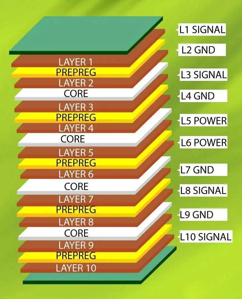
One of the key purposes of the HDI stackup design is confirming the relationship between signal layers and their reference planes.
A well-defined and clear reference structure of a HDI board is conductive to routing controll, stable electrical performance, and a more predictable layout of HDI PCB. If this initial relationship of signal layers and their associated reference planes is not properly established from the start, it will be very difficult to ensure the stability in the following design stage of HDI board.
The stackup design of HDI circuit board also has impact on signal paths that between different layers.
A reasonable HDI layer sequence can reduce unnecessary layer switches and also makes the overall HDI board’s structure more manageable.
What is noteworthy is that, if the layer of a HDI PCB is not properly planned, it can also leads to an increase in the complexity of the HDI stackup, even this HDI circuit board is fully routed.
Conclusion
For manufacturable HDI board,stackup design should be firstly regared as an electrical definition, not just a layer arrangement, HDI stackup determines signal reference structure and interlayer transition paths from the early HDI board design stage.
Besides the electrial issue of HDI board, the structural mechanics and stable manufacturability should also be considered in the design of HDI board stackup. As the stackup can also directly affects copper foil balance,lamination performance,material compatibility, and the overall producibility of the HDI PCB, these factors will be more critical when the phase turns from the HDI circuit board design stage to the real world production.
We will discusse about how stackup choices influence the manufacturability of HDI PCBs in another article, click here read more about Why Stackup Is the Starting Point of a Manufacturable HDI Board.
Request for a tech support
 | Download our design guidesfor better PCB designing and manufacturing These are some of the design guides designers and engineersdownload the most:
|
Proven by 7 industries, 4000+ customer projects
Please contact us at sales@knownpcb.com, ask for engineering support here or use the form below to reach out to KnownPCB | Get In Touch Today |