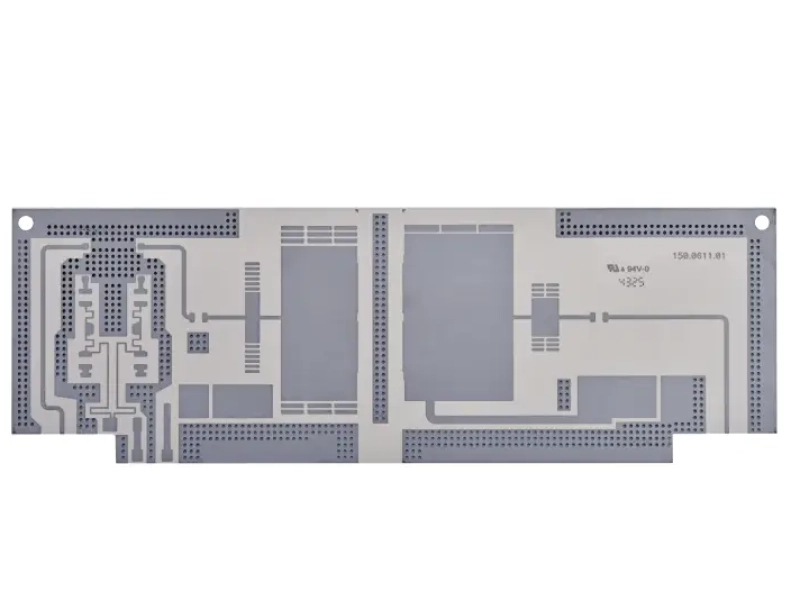
Start with a definition of Heavy Copper PCB: Heavy copper PCBs generally refer to boards with 3 oz (1oz≈35μm) copper or more on the outer or inner layers, that depending on the fabrication specification of heavy copper PCB.
Heavy copper PCBs are commonly used in high-power, high-heat-dissipation applications such as industrial power supplies, new energy vehicles, and medical equipment. For example, charging piles for new energy vehicles need to withstand high current surges. Common thin copper boards are prone to overheating and burning out. Heavy copper is like a backbone of the circuit, which can quickly conduct current, disperse heat, and improve the mechanical strength of the circuit board (resistance to bending and vibration).
However, heavy copper boards are not a case of the thicker the copper, the better.
“Improper design can lead to problems such as uneven heat dissipation, poor soldering, and soaring costs.” Ms Jiang said, the Manager of KnownPCB Production Department.
KnownPCB’s engineer wrote the article to start a discussion about the balance between requirement of copper weight and manufacturability.
The discussion below focuses on how to meet performance requirements of heavy copper PCB while also ensuring manufacturability (DFM).
1. Copper Foil weight Selection: Proper copper weight depends on the application so that lead a well-engineered configuration. More copper is not always the best solution. Key principle: The current determines the copper weight. Formula reference (simplified version):
As a rule of thumb, allowable current (A) ≈ Copper foil thickness (oz) × Trace width (mm) × 0.8 (Ambient temperature ≤40℃)
Typical example: 3oz copper foil + 3mm wide trace can withstand approximately 7.2A of current (depending on KnownPCB heavy copper manufacturing experience), which is sufficient for most industrial power supply scenarios.
Avoid: Copper foil thicker than 10oz will cause PCB bending and drilling difficulties. Unless there are special requirements (such as aerospace equipment), prioritize the mainstream 3-6oz specification.
2. Trace Design: Avoid current bottlenecks and localized heating. Trace width: Heavy copper traces should not be too narrow. As a recommendation, the minimum trace width for 3oz copper foil is ≥0.3mm (0.1mm is sufficient for ordinary thin copper). The larger the current, the wider the trace should be increased proportionally (for example, for 6oz copper foil carrying 10A current, the width is recommended to be ≥5mm).
Trace transitions: Avoid abrupt changes in trace width. (e.g., dropping abruptly from 5mm to 1mm). Use a "gradual transition" (length ≥ 3 times the width difference), otherwise a "current bottleneck" will form, causing localized overheating and burnout.
Heat dissipation optimization: Under high-power devices (such as MOSFETs), use "solid copper pours with thermal vias" (via diameter 0.8-1.2mm, spacing 2-3mm) to allow heat to be quickly conducted to the ground/power plane.
3. Heavy Copper PCB Via Design: Particular attention should be paid to via design in heavy copper applications.
Via diameter: The copper layer on the hole wall of the heavy copper board must match the thickness of the copper foil. A standard 0.4mm hole diameter cannot meet the electroplating requirements of 3oz copper foil. It is recommended that the minimum hole diameter be ≥0.8mm (hole wall copper thickness ≥20μm).
Number of vias: Do not use a single via on high current paths. For example, if a 3oz copper foil carries a 5A current, it is advised that using 2-3 vias in parallel (each via can withstand about 2-3A current) to avoid the vias overheating and melting.
Solder mask opening: Sufficient solder mask opening (0.2-0.3mm larger than the hole diameter) should be reserved around the via to prevent solder from clogging the via during soldering, which would affect heat dissipation and conductivity.
The core of DFM (Design for Manufacturability) is the design should align with the manufacturing process capability. For heavy copper boards, DFM focuses on solving the process challenges caused by heavy.
1. Copper Foil Etching: To avoid uneven etching, the minimum line width/spacing is: ≥0.3mm for 3oz copper foil and ≥0.3mm for line spacing (0.1mm is sufficient for thin copper); for 6oz copper foil, it might be worth considering that the line width/spacing be ≥0.4mm, otherwise inaccurate line width and short circuits may occur during etching. Solid copper pour design: For large areas of solid copper pour, a "mesh solid copper pour" (mesh spacing 2-3mm, line width 0.2-0.3mm) should be used to avoid the PCB board bending due to copper foil shrinkage during etching; if solid copper pour is required, thermal relief slots (width 0.5mm, spacing 10-15mm) should be reserved.
2. Heavy Copper PCB DFM Lamination process: To prevent "delamination and bubbling", the lamination sequence should be as follows: the heavy copper foil should be placed on the "outer layer" or "near the outer layer" to avoid being sandwiched in the middle and causing heat to be unable to dissipate; the copper foil thickness of the multilayer board should be symmetrical (for example, the top layer should be 3oz and the bottom layer should also be 3oz), otherwise it will warp after lamination. Substrate selection: Prioritize high Tg substrates (Tg≥170℃), such as FR-4 Tg170 and PI substrates, to avoid substrate softening and delamination during high-temperature welding (the welding temperature of heavy copper boards is usually 10-20℃ higher than that of thin copper).
3. Soldering process: The high thermal mass can be result in making soldering more difficult, it is priority to choose high power packages (such us TO-220, D2PAK) so that it causes insufficient wetting or cold solder joints.
Pad design: Pads on heavy copper should be 0.2-0.3mm larger than ordinary pads. In many cases, the pads for 0805 resistors are usually 0.8×1.2mm, but for heavy copper boards, 1.0×1.5mm is recommended to ensure a firm solder joint. Reflow soldering parameters: Heavy copper boards absorb more heat, so the reflow soldering temperature should be appropriately increased (5-10℃ higher than that of thin copper boards), and the holding time should be extended by 10-15 seconds to avoid cold joints.
4. Heavy Copper PCB Cost Control: The hidden value of DFM is to avoid over-design, for example, 1-2oz copper foil is sufficient in areas that do not require high current, and heavy copper is only used in critical paths to reduce material costs; Standardized dimensions: Use standard factory plate thicknesses (such as 1.6mm, 2.0mm) whenever possible. Special plate thicknesses (such as 3.0mm and above) will increase processing difficulty and cost.
Prioritize communication: Confirm process capabilities with the PCB manufacturer before design (such as maximum copper thickness, minimum hole diameter, and etching precision) to avoid design failures that prevent production.
Heavy copper PCB design comes down to three key considerations: matching copper weight to current requirements: avoid over-specify copper weight, select the mainstream specification of 3-6oz according to current requirements; avoid risks in details: gradual change of traces, parallel connection of vias, and compliance of trace width/spacing. DFM Priority: The design takes into account etching, lamination, and welding processes to reduce rework. Heavy copper PCB design introduces added fabrication constraints, but these can be addressed with sound electrical and process planning if you focus on two key factors.
Request for a tech support
 | Download our design guidesfor better PCB designing and manufacturing These are some of the design guides designers and engineersdownload the most:
|
Proven by 7 industries, 4000+ customer projects
Please contact us at sales@knownpcb.com, ask for engineering support here or use the form below to reach out to KnownPCB | Get In Touch Today |