Heavy copper PCB stands apart from normal types of PCB due to the unique nature of its raw materials, manufacturing processing and applications.
Compared with standard PCB structures, heavy copper PCB is more than just “extra thickness”.
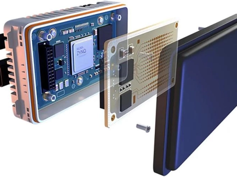
A specialist in heavy copper PCB manufacturing since 2008, we pride ourselves on tackling the industry’s challenging heavy copper PCB projects. Our expertise spans from robust multilayer power boards to extreme heavy copper designs, specifically engineered for the most demanding industrial and power electronics applications.
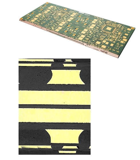
Inner: 5 oz / Outer: 3 oz copper Hole Wall Copper: ≥35 µm (1.4 mils) Min. Trace Width: 10 mil (Inner) / 8 mil (Outer) Dielectric Thickness: ≥0.08 mm (3.15 mils) Overall Thickness: < 3.50 mm, Rated Voltage: ≥ 2 kV • Stack-up: 6-Layer PCB • Finished Copper: 30 oz (Inners) / 6 oz (Outers) ,30 oz is extreme heavy copper • Laminate: Rogers / Arlon base material • Surface Treatment: Immersion Gold (ENIG) 12-layer heavy copper PCB
Layer Count: 12 Layers 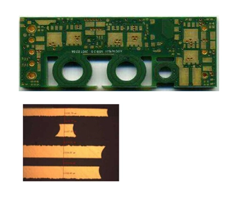
6-layer extreme heavy copper PCB
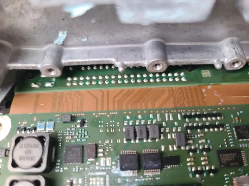
The specialized requirement on processing of heavy copper PCB which is characterized with copper thickness from 3OZ to 20OZ.
The thick copper PCBs with reinforced hole plating are designed for high-current applications. Multiple options of copper weight are available, from 18μm,35μm, 55μm and 70μm, 1oz (35μm) is settle to the most popular standard for thermally demanding applications.
KnownPCB’s manufacturing capabilities spans single-sided, double-sided, and multilayer PCB board up to 20 layers. Acting as a robust 'circulatory system' - characterized by high current-carrying capacity, superior heat dissipation, and enhanced structural integrity, heavy copper PCBs are the go-to choice for telecom power supplies, automotive electronics, industrial controls, and renewable energy systems.
Learn about detaild KnownPCB capability of heavy copper.
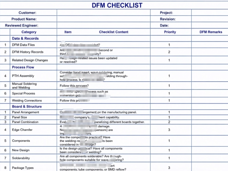
What are the challenges during heavy copper PCB fabrication or prototyping in KnownPCB workshop?
1.Overcome the challenge of chemical exchange to ensure a uniform result in etching processing
2.Address the bottlenecks of resin flow
3.Mitigate risks on Z-axis expansion stress
Now, that begs the question: when hardware engineers or PCB buyers select a heavy copper PCB manufacturer, what specific manufacturing capabilities should be on honing in on?
The following advanced heavy copper capabilities of KnownPCB can be a reference:
•Extreme Copper Weights: It is an industry-leading high-current solution to support both inner and outer layer finished copper thicknesses up to 1050µm (30oz).
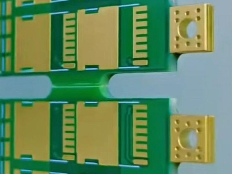
•Complex Interconnects: The production capabilities should be included Multilayer Blind & Buried Via structures for high-density, heavy-current designs.
•Advanced Via Filling: Reliable Resin or Conductive Copper Paste Plugging to ensure structural integrity and planar surfaces on thick copper layers.
•High-Reliability Materials: Full support for High-TG laminates to withstand rigorous thermal cycling.
•Enhanced Protection: Precise Solder Mask application with a thickness of up to 50µm for superior insulation.
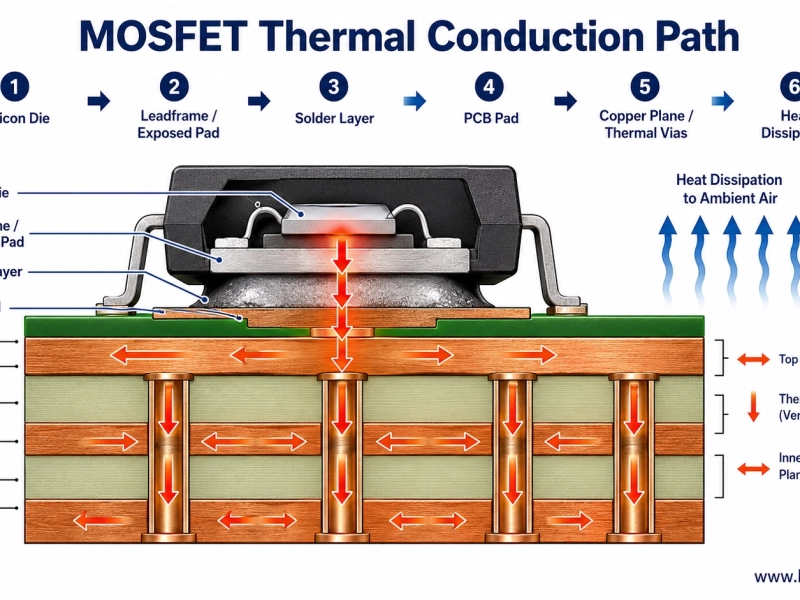
•Reinforced Plating: Guaranteed Hole Wall Copper thickness of 30µm+, ensuring robust vertical interconnects under high thermal loads.
Get custom thick copper PCB solutions from KnownPCB for power electronics, industrial control, and high-current applications. We support prototype, low-volume, and multilayer heavy copper PCB manufacturing.
Request for a tech support