Get A Quote
CN
Quick Navigation
System-Level Reliability Risks of Extreme Heavy Copper Trade-off Advice about Heavy Copper PCB FAQ about Heavy copper PCB trace with design
Heavy copper is helpful for high-current PCB that involves a trade-off in electrical performance and PCB fabrication limits, meanwhile comes with a catch cause by the increased challenges at the production and quality risks. The rules of trace design for heavy copper PCB are a huge wake-up call for the PCB layout engineers coming from a standard 4-layer digital background.
Standard layout rules, such as 4mil trace width and spacing, will be a textbook mistake that the heavy copper PCB layout engineer blindly apply fine lines on heavy copper PCB for high current application. It is not workable.
In this guide, we will look at the actual limits of heavy copper routing and manufacturing so that avoid to the endless revision.
If you are running a prototyping heavy copper PCB, you can try to push the PCB fab house beyond their standard PCB process capability, but the heavy copper PCB is on a tight schedule, strictly play by these manufacturing rules and stay well in their comfortable zone to keep a stable production yields. It will be also a guaranteed way to a on-time delivery.
| Finished Copper Weight | Trace Width and Spacing (W/S) |
|---|---|
| 3 oz | 8/8 mil |
| 4 oz | 10/10 mil |
| 5 oz | 15/15 mil |
| 6 oz | 18/18 mil |
The precise production of trace in heavy copper PCB comes down to the etching limitation, copper foil weight, plating uniformity across board and the resolution of the photoresist.
Due to the increased copper foil thickness(such as 2oz, 3oz or above), undercutting, one of the heavy copper PCB manufacturing processing, causes high topography ,that becomes much more severe during etching when , resulting in a non-uniform trace profile that makes fine-line features (<50μm) extremely difficult to resolve. This means the resulting surface topography, plating variations, and pattern density effects compromise dry film adhesion and pose severe challenges for solder mask clearance.
Submit for a Free Heavy Copper DFM Review to Reduce rework
The etchant dissolves the metal vertically while also eating away at the trace edges horizontally during the etching process.
Single-sided undercut is often estimated at approximately 15%–20% of the copper thickness under standard wet etching conditions.
According to IPC-2221, it will be appreciated that etch compensation is treated as a proactive design responsibility, rather than a belated CAM fix. Heavy copper PCB designers are suggested to pre-load these allowance margins into their EDA tools based on copper weight and etch factors.
But at the side of heavy copper PCB manufacturer, in practice, the exact Etch Factor (EF) and final trace tolerances are really dependent on the heavy copper PCB factory’s chemistry setup, spray pressure, layout density, and the etch compensation. Thus, this ratio is also by no means a fixed constant.
| Base Copper Thickness | 8 μm | T oz | H oz | H oz | 1 oz | 1 oz | 2 oz | 3 oz | 4 oz | 5 oz |
|---|---|---|---|---|---|---|---|---|---|---|
| Finished Copper Thickness | 1 oz | 1 oz | 1 oz | 1.5 oz | 1.5 oz | 2 oz | 3 oz | 4 oz | 5 oz | 6 oz |
| Mass Production W/S | 3.5/3.5 | 3.5/4 | 4/4 | 5.5/5.5 | 6/6 | 7/7 | 9/9 | 12/12 | * | * |
| Sample W/S | 3/3 | 3/3.5 | 3.5/3.5 | 4/5 | 4/5 | 6/6 | 8/8 | 10/10 | 15/15 | 18/18 |
| Compensation Value | 0.5–1.2 | 0.8–1.5 | 1.4–1.7 | 1.7–2.2 | 1.7–2.4 | 2–3 | 3–4 | 5.0–6.5 | 7.0–9.0 | 11–13 |
| Minimum Spacing after Compensation, including Square PAD to Trace | 3 | 3 | 3 | 3.3 | 4 | 4 | 5 | 6 | 8 | 8 |
| Round PAD to Trace Spacing after Compensation | 2.6 | 2.6 | 2.6 | 3 | 3.3 | 3.3 | 4 | 5 | 6 | 6 |
The below formular of Etch Factor is introduced by heavy copper PCB factory , which purpose is the ratio of downward etching to lateral etching.
The higher the F value, the better the heavy copper PCB factory's control over the chemical etching process.
F =H/U(ratio of vertical etch depth (H) to the lateral undercut per side (U)
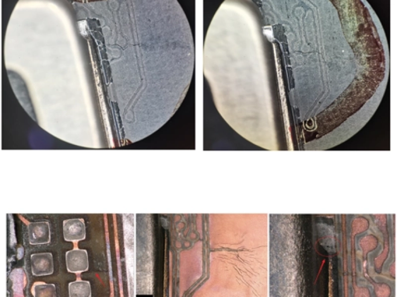
It will cause incomplete etching when spaces are too narrow. Basically, the chemical finishes off the bottom of your traces before it can fully etch through the center area, leaving you with a mushroom-shaped wire that may result in trace lifting at the laminate. Once your trace shrinks beyond 10%(Line Width Conformance), you will fail IPC-6012 inspection immediately.
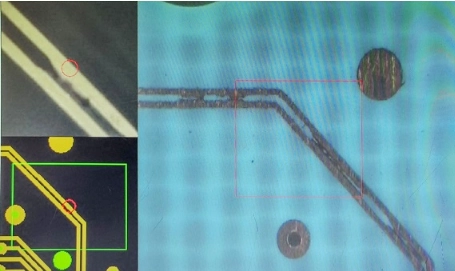
Unetched Copper in Heavy Copper PCB
The limitation of Etching process: etching process significantly runs into a bottleneck at the minimum trace width. Trying <0.2mm on 3oz will push your heavy copper PCB manufacturer to enter an aggressive window during PCB manufacturing, the manufacturability of heavy copper PCB should be confirmed by PCB manufacturer before DFM if you don’t want to go back to the drawing board.
Ask for a tech support at estimating manufacturability of heavy copper PCB
Going beyond manufacturing constraints of heavy copper PCB fabrication, heavy copper imposes severe long-term reliability challenges at the system level.
Thermal/Mechanical Stress: The structural rigidity of thick copper, coupled with the severe CTE mismatch against the FR4 matrix, aggressively amplifies Z-axis expansion during thermal cycling, this routinely leads to delamination or inner-layer interconnect (ICD).
Environmental Degradation & High-Voltage Insufficient Isolation: Any solder mask pooling at the steep trace valleys paves the way for moisture ingress, significantly escalating the risks of Electrochemical Migration (ECM) and CAF failure under high-voltage bias.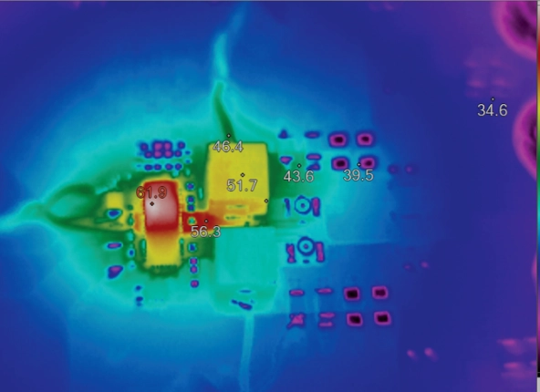
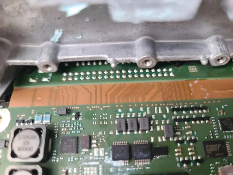
Thermal image of the device under a 20 A load
Laminate Delamination Risks: During thermal excursion, extreme copper thickness (≥5oz) drives localized Z-axis shear stress up to 18 MPa in certain stack-ups, due to the CTE mismatch between heavy copper foil and resin matrix. Once this localized stress exceeds the material's inherent Interlaminar Shear Strength (ILSS) (typically 15 MPa), interfacial peeling is inevitable. However, adopting low-CTE base materials, optimized dwell times in split-lamination cycles, and plasma activation can reduce the defect rate to below 0.3% in validated production condition.
Signal Integrity Degradation: At high frequencies, a ±2mil etching tolerance directly translates into severe impedance discontinuities, triggering parasitic reflections. Under high-frequency operation, the impedance jump at thick-to-thin transitions, distorted return paths, and via stubs severely degrade noise margins and close the eye diagram. Standard remedies involve backdrilling, trace tapering, and monitoring via specialized coupon testing.
Interfacial Contamination & Adhesion Degradation: If moisture gets in(also, moisture ingress), coupled with high concentrations of sulfide contamination on the inner-layer brown oxide bond film, severely degrades the copper-to-resin interfacial adhesion strength by over 30%. Over time, this leads to Conductive Anodic Filament (CAF) leakage or makes the copper foil delamination. To safeguard the laminate architecture, using plasma cleaning and nano-silane can keep it perfectly clean and boost the peel strength to a solid 1.8 N/mm.
In high-power application, if the copper thickness is not non-uniform electroplating, the current will squeeze into the thin spots and spike up the density. This Electromigration, leaving hidden holes or growing tiny whiskers (also call void formation) that will eventually propagates into a catastrophic open-circuit failure.
Inspection Blind Spots during PCB QA/QC process: extreme copper thickness (>5oz) drastically intensifies X-ray absorptionbecause it blocks the radiation. This means the thick copper will completely mask any tiny cracks or hidden voids underneath, making them invisible to your QC team. The high specular reflection from the steep, vertical copper topologies creates extreme optical glare and shadowing, severely compromising the AOI system’s contrast algorithm and failing to recognize localized solder mask voiding.
When your system’s continuous operating current exceeds 100A and routing density restricts space clearance, do not simply resort to brute-force stacking of full-board copper thickness to 6oz or 8oz heavy copper PCB. At that point, your yields will take a cliff-dive while costs skyrocket. The best engineering practice is to use a 2oz/3oz multilayer board as a foundation, then introduce embedded copper blocks in localized high-current paths, or directly integrate 3D busbars. Use architectural synergy to bypass the physical limits of a single process.
Increasing copper weight does improve heavy copper PCB current-carrying capacity, meanwhile it takes etching compensation much more risks. Take 5oz copper (approximately 175 μm) for instance: if the Etch Factor (EF) is 3.0 (a solid industry standard), the single-sided undercut is about 58 μm, or 2.3 mil. Therefore, the heavy copper PCB production artwork must pre-load a ≥4.6 mil total compensation margin. For a target 15 mil trace, the photo-mask must be drawn at 19.6 mil.
If the heavy copper PCB factory's EF drops to 2.0 (low-end shop), the undercut doubles, shrinking your 15 mil trace down to 10.4 mil in the real world, which completely tanks your current capacity by over 40%. Therefore, the link between copper thickness and spacing is a delicate balancing act within the etching process window—heavy copper demands a high-EF process, or the design is dead on arrival.
Ask for a guideline about heavy copper PCB trace design
* heavy copper pcb minimum trace width
thick copper routing clearance limitations
3oz copper pcb minimum spacing
why fine lines fail on heavy copper
A: Applying standard fine-line spacing (like 4mil) to heavy copper profiles is technically unworkable. Thick copper foil (3oz to 6oz) drastically increases vertical topography, amplifying isotropic side-etching (undercutting). If your trace clearances are too narrow, the etchant aggressively eats away at the conductor walls horizontally before fully clearing the trench center, leaving an unstable mushroom-shaped trace profile that triggers incomplete etching or trace lifting.
A: When your system’s continuous operating current exceeds 100A, relying solely on standard formulas to expand line widths becomes unworkable due to routing space constraints. Directly escalating full-board copper thickness to 6oz or 8oz to compensate for narrow widths is structurally inefficient, causing production yields to degrade sharply while manufacturing costs scale exponentially. To bypass the physical etching limits of full-board heavy copper, the best industry engineering practice dictates architectural synergy:
* Embedded Copper Blocks: Utilize a stable 2oz or 3oz multilayer PCB as your foundation, and selectively integrate localized massive copper blocks directly into the stack-up along high-current paths. This allows you to carry extreme currents locally without widening traces across the entire layout.
* 3D Busbar Integration: Route high-power paths off the surface of the board by directly integrating vertical 3D copper busbars. This architectural hybrid completely removes the massive width requirement from your standard PCB routing layers.
A: Directly escalating continuous full-board plating to 6oz or 8oz is a highly inefficient strategy that causes manufacturing yields to take a cliff-dive while skyrocketing production costs. The proven industry alternative is architectural synergy: use a stable 2oz/3oz multilayer board as your core foundation, and then selectively integrate Embedded Copper Blocks or 3D Busbars along localized high-current paths to safely bypass the physical etching limits of a single chemical process.
A: Measuring the finished copper thickness tolerance on extreme copper profiles (>5oz) effectively requires moving beyond standard surface-level micrometer gauges. Due to the inherent physics of isotropic chemical etching, heavy copper traces do not possess perfectly vertical walls; instead, they exhibit a pronounced trapezoidal cross-section or mushroom profile driven by lateral undercutting.
To achieve reliable, IPC-compliant thickness conformance verification, standard industry quality control dictates a combination of the following advanced non-destructive and destructive testing (NDT/DT) methodologies:
Micro-Sectional Metallographic Analysis (Destructive Testing): This is the ultimate baseline reference for heavy copper validation. By potting, cutting, and polishing a specialized coupon test piece, QA teams can precisely measure the true vertical copper thickness (H) alongside the exact single-sided undercut (U) under a calibrated optical microscope to verify the real-world Etch Factor (F =H/U). Eddy Current Testing (Non-Destructive Testing): Handheld or automated electromagnetic induction (eddy current) gauges are highly effective for measuring base and finished foil thickness prior to solder mask application. However, probe placement must avoid localized constricted cross-sections where plating thickness variations typically manifest.
* High-Resolution X-ray Fluorescence (XRF): While extreme copper weights (>5oz) can severely attenuate and block low-energy radiation—making internal sub-surface micro-cracks invisible—calibrated high-energy XRF systems remain effective for verifying localized surface plating tolerances on open pads or trace flats before the structural topology interferes with the detection window.
Submit for a Free Heavy Copper DFM Review