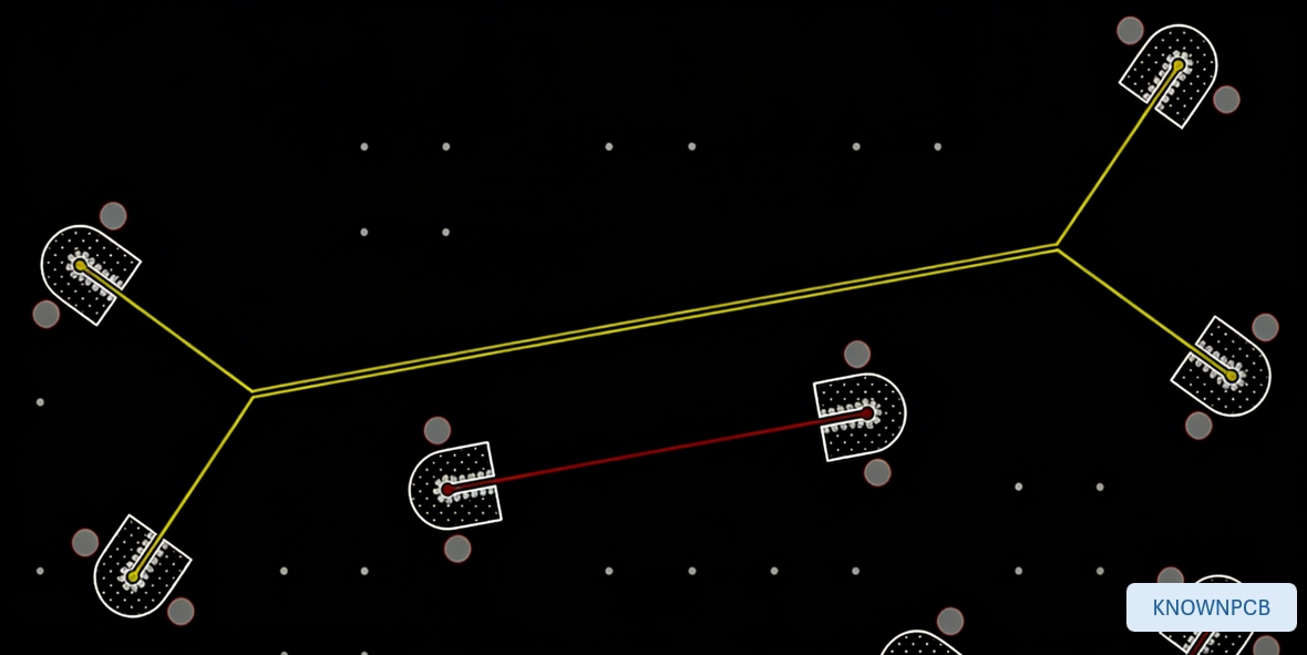
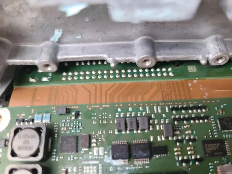
Test Vehicle / DUT: Top Layer Differential Pair
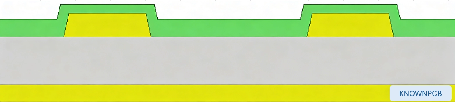
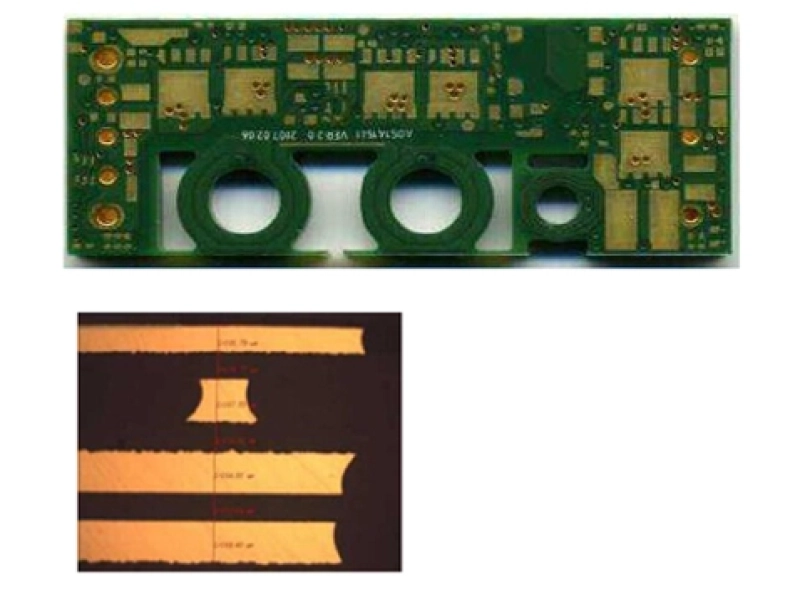
Modeling Basis: Microsection Analysis and 3D Structural Models
Thus, the influence of PCB green oil thickness on high-speed signals.
There was a case for this :
100Ω differential microstrips on M6 laminate (top layer) with green solder mask:
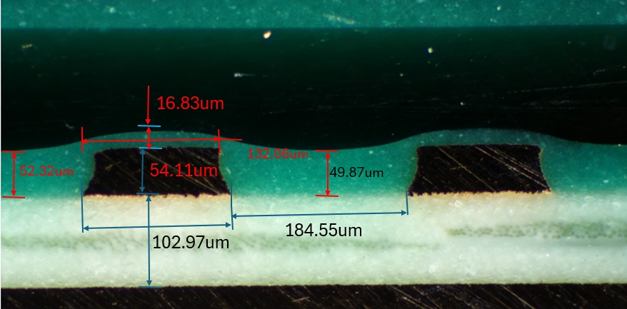
The PCB cross-sectional analysis provides a comprehensive assessment of the fabrication build-up,
accounting for trace geometry, dielectric height, copper surface profile, and solder mask deposition.
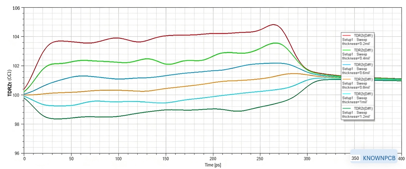
Check out this animation showing how solder mask thickness—ranging from 0.2 to 1.2 mils—affects high-speed signal integrity on the top layer.
Scaling the PCB solder mask thickness from 0.2 mil to 1.2 mils results in a differential impedance drop from 104Ω to 98Ω, exceeding a 5Ω total variance.
Another critical parameter affected is insertion loss.
The PCB test data shows that scaling the solder mask from 0.2 to 1.2 mils leads to a nearly 20% penalty in loss performance, emphasizing why precise mask control is vital for high-speed designs.
March/20/2026Automotive Multi Camera System Demands and Challenges in PCB Process
December/05/2025Automotive Camera Modules (ADAS) HDI PCB Solution
April/09/2026Heavy Copper PCB Projects
July/10/2026Prototype PCB Assembly vs Low Volume PCB Assembly
May/27/2026DFM for PCB with Large-Footprint Components
