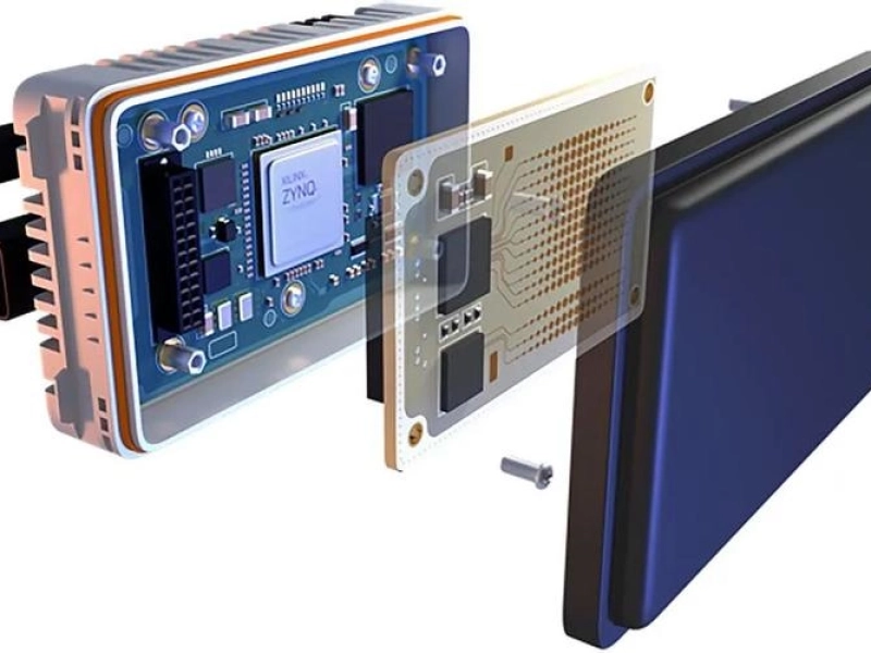
MOSFETs and PCB/SMT Integration
A MOSFET is not just a “plug-and-play” component. More often than not, there are many figurations should be included, its electrical performance, thermal behavior, package type, the design of PCB copper and stencil aperture, reflow profile, X-ray voiding, ICT/FCT testing, and mass-production yield. Regarding the robust power MOSFETs, many MOSFET-related failures are caused by poor PCB layout or SMT processes, that act as a bottleneck to degrade the heat dissipation, current handling, solder-joint reliability, or long-term production stability.
1. The Key Role of MOSFET, from Design, PCB Layout, SMT Process, and Production Readiness
A. Device Selection: SMT Risk Management
Engineers evaluate more than VDS, ID, RDS(on), Qg, SOA, and avalanche capability when selecting a MOSFET, meanwhile review the PCB design rules and the available SMT process capability.
Common MOSFET Package & PCB/SMT considerations include:
| MOSFET Package | PCB/SMT Relevance |
|---|---|
| SOT-23 / SOT-223 | It is simple to assemble, but limited in thermal performance. Heat dissipation depends heavily on pad design and copper area. |
| SO-8 / PowerPAK / LFPAK | Commonly used for medium- to high-current applications. Thermal performance depends on large leads or bottom thermal pads, making stencil design and void control critical. |
| DFN / TSON / TDSON | Features of compact and low in thermal resistance, but sensitive to placement accuracy, stencil aperture design, land-pattern design, and X-ray inspection. |
| TO-252 / DPAK / D2PAK | It is vital to evaluate high thermal mass packages that require careful evaluation of reflow profile, solder wetting, thermal copper area, and current paths. |
Summary: KnownPCB notes: According to the LFPAK MOSFET thermal design guidance issued by Nexperia, the conduction loss, switching loss, and avalanche loss all contribute to the total power-loss model, where PCB design limits the devices’ actual power tolerance.
B. Schematic Design: MOSFET Usage Drives PCB Requirements
MOSFETs are typically designed for switching, synchronous rectification, load switching, motor driving, hot-swap protection, and reverse-polarity protection in a PCB layout. Each application enables PCB layout and SMT process control different constraints.
| Application | PCB/SMT Focus on The Followings |
|---|---|
| DC-DC synchronous rectification | Minimized switching loop, gate loop control, SW-node area, EMI, and heat spreading |
| Motor drive / H-bridge | High-current path design, current sharing between parallel MOSFETs, thermal copper area, and solder-joint reliability |
| Battery protection / load switch | RDS(on)-related heating, drain/source copper area, and overcurrent testing |
| Reverse-polarity protection | SOA, transient thermal stress, copper thickness, and via current capacity |
| High-frequency switching | Gate resistor selection, Kelvin source routing, parasitic inductance, and layout-related ringing |
Therefore, we shift the focus from a sufficient current rating in MOSFET to other package’s requirements, it is about whether the assembled PCB can support the required thermal performance, current capacity, and soldering reliability after the device is mounted.
C. MOSFET performance is related to PCB layout
The typical thermal path for power MOSFETs is:
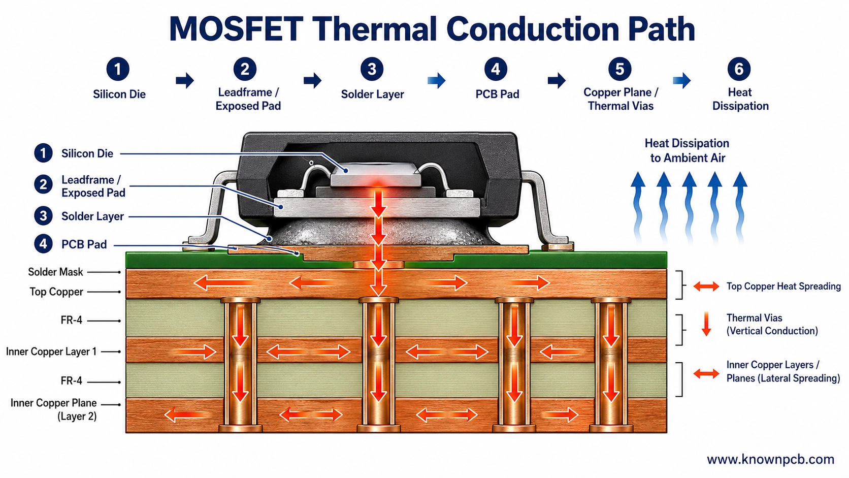 thermal path from silicon die to PCB copper planes and thermal vias
 PCB layout directly impacts on this thermal path.
Key layout considerations
- Drain/source high-current paths should be short, wide, and low in impedance.
This reduces voltage drop, with the benefit to preventing localized heating and current crowding. - Thermal copper area is necessary and sufficiency, but more copper does not always produce proportional improvement.
ROHM’s PCB thermal design guidance indicates that the benefit of reducing thermal resistance eventually becomes non-linear and reaches diminishing returns. - Thermal vias dictate the thermal path
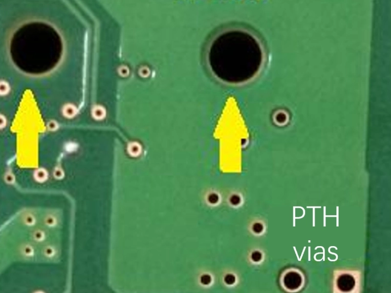
For MOSFETs with exposed thermal pads, the number, diameter, pitch, and via-plugging method all affect both thermal conduction and solder voiding. - Thermal vias are gatekeepers.
Engineers carefully optimize the number, diameter, pitch, and via-plugging methods of these vias within the thermal pad to to strike a balance between thermal conductivity and solder voiding. - Large pads must not become a source of SMT defects.
Large pads usually lead to risks or failures, like insufficient soldering, component floating, solder voids, solder beading, or nearby tombstoning if the stencil and reflow process are not properly controlled. - The gate loop must be kept clean.
The quality defects, like ringing, false turn-on, EMI, and higher switching losses if long gate traces or poor source-return paths. In practice, these issues often appear as MOSFET overheating or premature failure.
D. PCB DFM Stage: the capability of PCB Factory
MOSFET-related DFM checks should include the following items:
| Item | Inspection Focus |
|---|---|
| Copper thickness | Whether 1 oz, 2 oz, or 3 oz copper is sufficient for the required current and thermal performance |
| Trace width / copper area | Whether the high-current path is wide enough and free of bottlenecks |
| Thermal vias | Via diameter, spacing, plugging method, solder-mask coverage, and resin-filled via-in-pad capability |
| Surface finish | Compatibility of OSP, ENIG, or HASL with fine-pitch packages and large thermal pads |
| Solder-mask bridge | Whether solder-mask definition can be maintained for DFN/TSON fine-pitch pads |
| Panelization direction | Thermal uniformity of large MOSFET areas during reflow |
| Warpage risk | Effects of heavy copper, large copper pours, and local thermal-mass imbalance |
Summary: KnownPCB Summary: we cannot simply define that thermal-pad vias, solder wicking into vias, voiding, and via-plugging methods are far from being just PCB issues. Rather, they are assembly-reliability concerns jointly determined by MOSFET package design, PCB fabrication, and SMT reflow conditions.
E. SMT Process Stage: Soldering Quality Directly Affects MOSFET Thermal Resistance and Reliability
Common process risks of MOSFET during SMT process:
| Process Step | MOSFET-Related Risk |
|---|---|
| Solder paste printing | Excessive or insufficient solder volume on large pads; improper stencil aperture design |
| Placement | Offset or rotation of DFN/TSON packages; bottom pads cannot be visually inspected |
| Reflow soldering | Insufficient heating of high-thermal-mass MOSFETs; overheating of nearby small components |
| X-ray inspection | Voiding, solder bridging, or open solder joints under exposed pads |
| AOI | Visible lead soldering defects, misalignment, insufficient solder, or excessive solder |
| ICT/FCT | On-resistance, voltage drop, switching function, and temperature rise |
| Burn-in / thermal cycling | Solder-joint fatigue, thermal-resistance drift, and intermittent failures |
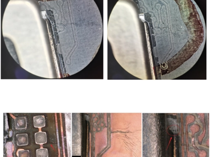
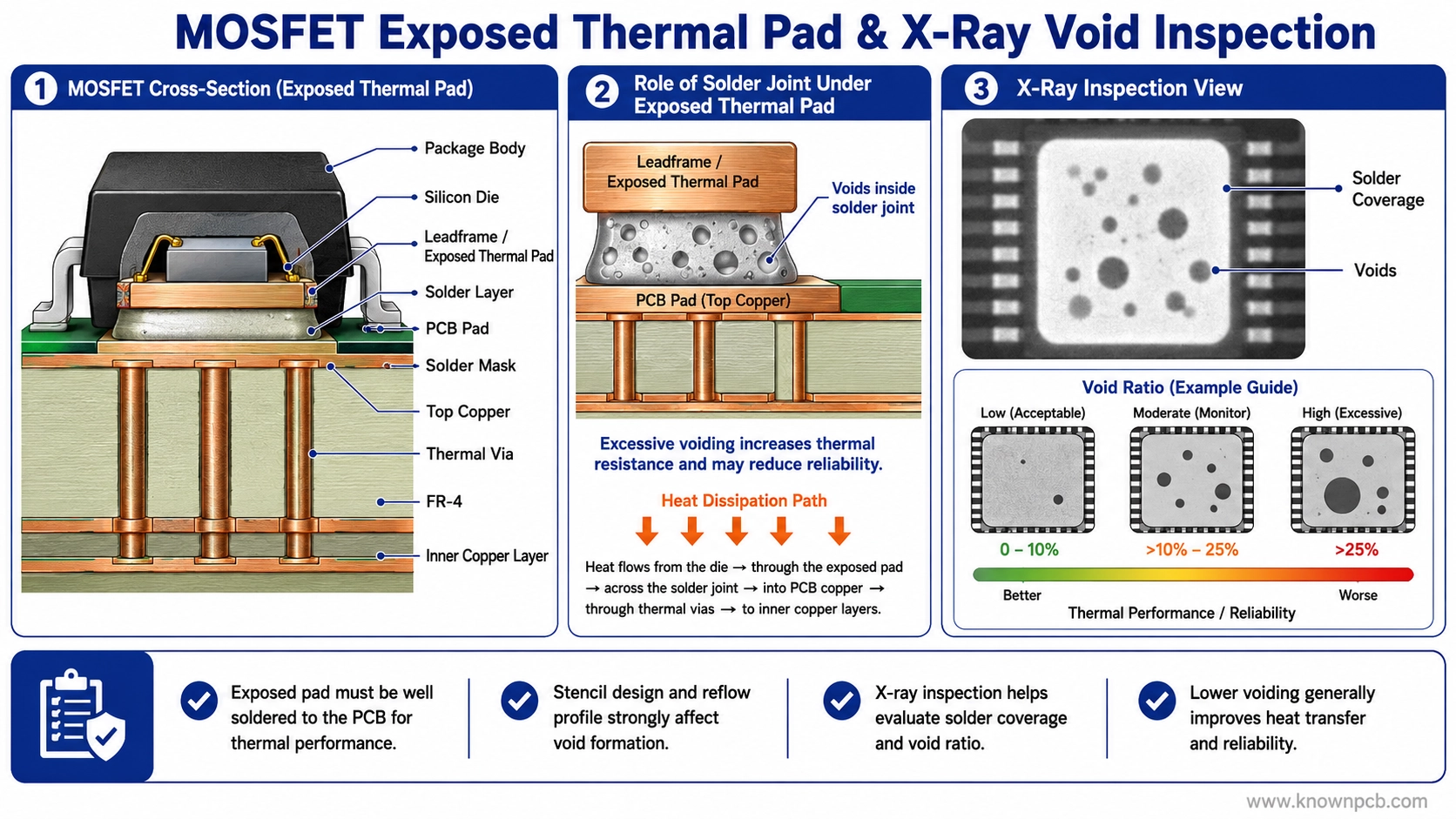 exposed thermal pad, solder layer, solder coverage, X-ray voids, and void ratio
 KnownPCB emphasizes: that the packages with exposed pads designed for thermal enhancement must have the exposed pad directly soldered to the PCB.
F. EVT / DVT / PVT: Verifying Whether Design Margin Can Be Reproduced in Production
We must look beyond whether the prototype works simply or passes functional test before go-to-production. The following evaluation list for reference:
| Stage | MOSFET/SMT Evaluation Focus on |
|---|---|
| EVT engineering prototype | MOSFET temperature rise, switching waveform, ringing, efficiency, and abnormal operating conditions |
| DVT design validation | High/low temperature, full load, short circuit, surge, hot swap, and aging tests |
| PVT pilot production | SMT yield, X-ray voiding rate, solder-joint consistency, and rework rate |
| MP mass production | Cpk, AOI/X-ray defect trends, FCT failures, and field failure rate |
Special attention should be paid to the checking points:
- Whether the MOSFET temperature is a sufficient margin under full load.
- Validate the temperature rise remains consistent across different PCB lots, reflow ovens, and solder-paste batches.
- Whether voiding under exposed thermal pads is controlled within an acceptable & safe range.
- Confirm that high-current solder joints show insufficient solder, open joints, cracks, or other reliability risks.
- Whether MOSFET failures are caused by electrical overstress, thermal-design weakness, or soldering defects.
Final Summary: KnownPCB NOTES: MOSFET power dissipation varies with copper area, PCB layer count, and via conditions. This means the PCB must be validated as part of the thermal system before mass production, rather than relying only on isolated datasheet parameters.