Get A Quote
CN
As a leading PCB manufacturer serving global customers since 2008, KnownPCB would like to share real-world insight: a classic HDI failure analysis, it is a logical method with clear steps for checking the root cause of HDI microvia cracking:
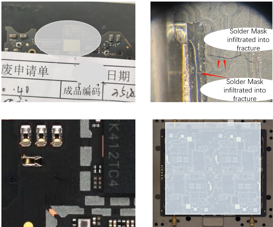
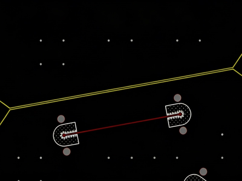
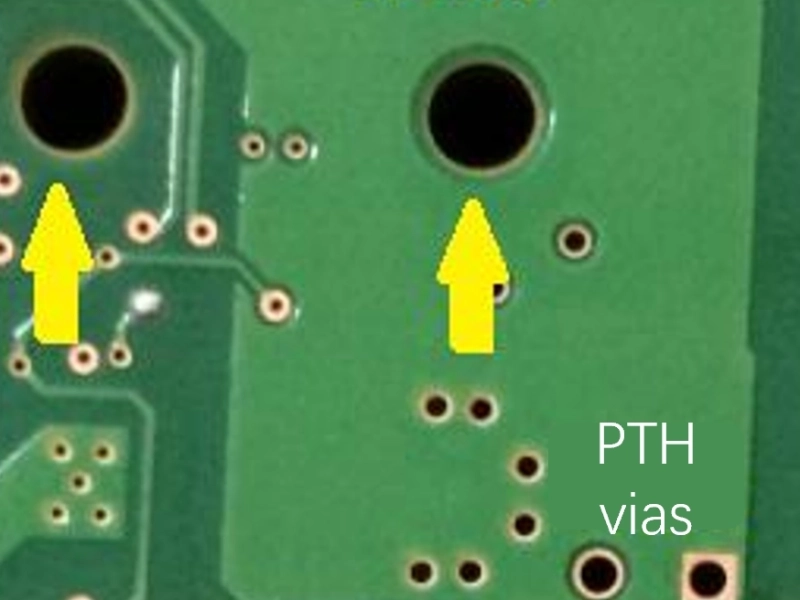
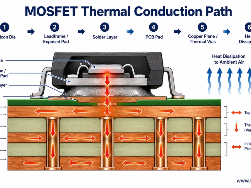
One of the most prevalent failure case in PCB failure analysis(FA): Microvia Cracking Post-Reflow
Post-reflow functional failures in a batch of HDI boards were traced to electrical opens in the HDI BGA area via flying probe inspection.
Analysis steps:
Root Cause:
• Process Optimization: Added ultrasonic DI water rinse stages for a deeper cleaning.
• Upgrade Plating: Used pulse plating for tougher, more flexible copper.
• Stricter Compliance: Enforced a strict ban on all chlorinated substances at the source.
• Data-Driven QC: Introduced MSA to ensure consistent cleaning results. Outcome: No failures recorded after 1,000 thermal shock cycles (-55°C/+125°C).
Understanding the PCB manufacturing process is more than just building a functional board. It empowers you to design within fabrication limits during early design, sidestep risks during component selection, and lock in the optimal process window before mass production.
Request for a tech support
KnownPCB Production Lines
KnownPCB Industry Solutions
Submit Your Gerber
Request Stackup Review
March/10/2026PCB Solder Mask Function and Major Influence
March/20/2026Automotive Multi Camera System Demands and Challenges in PCB Process
April/23/2026Through-Hole Assembly Capabilities & DFM Checklist
May/15/2026MOSFETs and SMT Integration
December/06/2025What Are The HDI Board Risks for Radar Modules
