Summary:
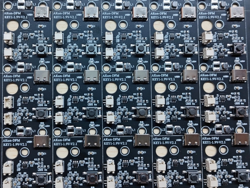
Single sided PCB board is the most basic type of printed circuit board. This article includes the definitions, benefits, suitable application field and some design tips of single sided copper PCB board. At last, frequently asked question about single sided flexible PCB board and double-sided PCB board are also mentioned.
1. What Are Single Sided PCB Board?
Single sided PCB board is the most basic type of printed circuit board. Specially, only one side of the substrate covers copper foil with a conductive circuit pattern. The other side is an insulating substrate only with solder mask and spraying layer.
Core structure and principles of single side PCB board is not too complex. Because of single-layer routing, all electrical traces and pads must be completed on the same copper layer. Conductors wire should not cross each other. If we can avoid wire crossing, jumper wires strategies can solve the problems. Its electronic components usually stay on the side which there is no copper foil. And the pins of them pass through the holes in the substrate and then connect to the other side by welding. As for the drilled holes on it, they play the role of mechanical fixation but not the inter-layer electrical connection.
2. When Should I Use 8 Layer PCB Stackup?
2.1 Low Manufacturing Cost
Single side PCB Board only have one layer of copper foil. And the substrate material, FR-1 paper-based phenolic resin, cost less money than others. Also, no extra expensive hole metallization process, like plating and electroplating, leads to a good unite price.
2.2 Simple Production Process
The process only includes graphic transfer, etching, and non-metallic hole processing. The manufacturing quality can be very stable. So it is suitable for large-scale standardized production.
2.3 Short Lead Time
Fewer processes save lots of manufacturing time. For example, product line can skip inter-layer alignment or metallization steps, compared to double-side PCB and multiple layer PCB.
2.4 Low Design and Maintenance Difficulties
One-layer wiring directly simplifies the design rules. Even though some cases involves cross-coupling, the design logic is still easier. Last, when troubleshooting, the layout of components and circuits is clear for checking and understanding, especially the soldering points.
3. What Is the Single Sided PCB Board Application?
- l Consumer electronics device like remote control, calculator, electronic watch, radio, basic model printer is very suitable to use single sided PCB. These products have a common similarity, which function is very simple.
- l Besides, single side PCB board can be also applied in household appliances, such as electric fan, rice cooker, coffee machine, desk lamp, and washing machine.
- l The lightning and battery products needs a relatively regular circuit design. So single sided PCB board can meet this requirement. For example, we frequently receive single sided PCB in the field of mobile phone chargers, power adapters, and LED lighting driver boards.
- l Industry and Internet of Things. Simple sensors, relay control boards, and low-cost wearable devices can match single sided PCB. In these fields, single-panel designs offer cost-effective solutions for simple monitoring or control functions.
4. How to Select Proper Single Sided PCB Board Manufacturing and Assembly Services?
4.1 Manufacturing Capability
For single side PCB board, there is no requirement for inter-layer alignment. We can focus on checking the manufacturing ability of the minimum line width and spacing (usually ≥ 10 mils can meet most requirements), hole diameter accuracy, and copper thickness tolerance. If possible, don’t choose manufacturers that are only proficient in HDI or high multi-layer boards. Because their production line scheduling priority is low, and the unit price is inflated.
4.2 Material Base and Surface Treatment
Single panels cost less money. Some of supplier may replace good products with substitute inferior ones. It is necessary to clearly ensure the FR-4 grade (such as Tg 130℃ or 150℃) and copper foil type (electrolytic/roll-forming). Also, don’t forget to confirm the solder mask ink brand. We recommend lead-free tin spraying (high cost-effectiveness) or OSP for single side PCB board surface treatment rather than gold plating, because it has high cost-effectiveness.
4.3 Good Testing and Quality Assurance Ability
Faults in single panels often result from open circuits or short circuits. In some cases, we can require suppliers to perform 100% flying probe testing or AOI full inspection, if the lead time is not urgent. Also, choosing factory which follow IPC-A-600 Class 2 is also a good idea.
5. Design Tips for Single Sided PCB Board
5.1 Prioritize Layout over Wiring
Firstly, we can make sure the same component orientation. All SMT components usually parallel to the board edge to accommodate wave soldering or single-sided reflow processes. This can greatly avoid protrusions and displacements. Another tips for layout is reserving jumper space. If cross-crossovers is necessary, we can define the jumper component during the schematic design stage and reserve physical installation positions during PCB layout. Try not to totally trust in software to automatically route wires. If you want to make the design easier for yourself, you can give priority to placing connectors, connectors, and high-pin-count ICs first to ensure sufficient wire-wrapping space for their outgoing leads. This greatly avoid being blocked by small components later.
5.2 Routing strategy: Avoid Crossings and Loops
A good routing strategy must prohibit right angles and sharp angles. We highly recommend 135°or arcs to reduce signal reflection and etching residue risks. The reason is that single-sided wiring is more sensitive to line width and spacing tolerances.
Sometimes, we also have to consider minimizing circuit area. Due to the lack of a complete ground plane, the signal return path is long with high impedance. Critical signals, such as clocks and resets, should run close to power or ground lines to artificially construct a low-impedance return path. This can greatly reduce EMI.
Many good designers also prefer broadening power and ground lines. Single sided copper clad PCB board contains no inner-layer power plane, so we recommend widening the main power and ground lines. For example, some designers arrange more than 20mil-space based on current carrying capacity. Adopting a tree-like structure for the layout can also avoid uneven voltage drops caused by chain connections.
5.3 OEM Process Compatibility
We can see wave soldering compatibility as the priority. If using a mixed assembly of through-hole and surface-mount components, the axial direction of the through-hole components should keep perpendicular so as to the transfer direction. Besides, if the IC pins such as SOP/QFP is more than 1.27mm, we can consider wave soldering. This can save lots of cost, compared to use a separate reflow process.
Then, if we want to improve the prevention ability of solder joints cracking, do not place heavy components near the board edge, mounting holes, and connectors.
If the current of your single sided copper PCB board exceed 1oz (35um), do ask the OEM factory whether they can do 2 oz. Because most common copper is around 1 oz. In addition, please do adjust the line width if any design changing. This can ensure no short circuit.
5.4 Design Appropriateness Consideration
Single side PCB board suits simple PCB layout. Only when the number of components is lower than 50 with no BGA or QFN bottom pad components, single sided copper PCB board have cost advantages. If some cases involve complex design, it is not recommendable to do a forced design simplified or space-saving. This may lead to bad quality.
6. Frequently Asked Questions
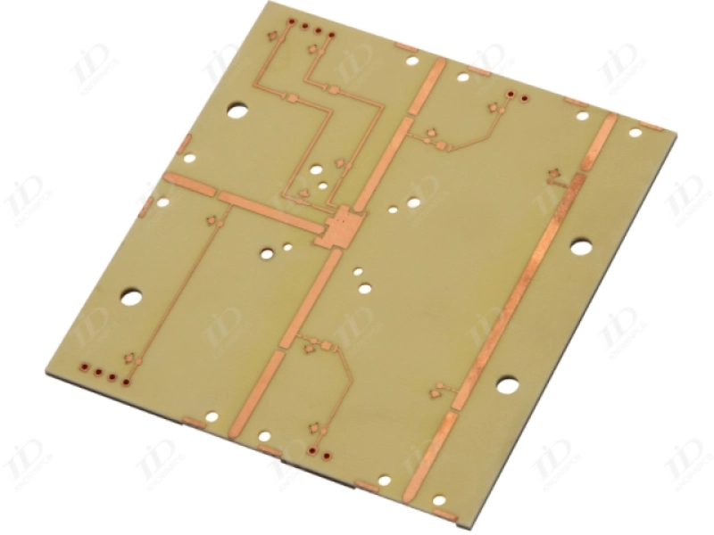
6.1 Do You Also Have Double Sided PCB Example?
(插入图片)
Yes, we do have double sided PCB example. As for PCB double-sided boards, copper plating covers both sides. The via holes allows electrical connections between layers. They are small holes filled or coated with metal. We KnownPCB can provide double-sided PCB as prototype or OEM batch products. If any inquiry, please feel free to contact us.
6.2 What Is Single Sided Flexible PCB Board?
Single-sided flexible PCB is the most basic structural type of Flexible Circuit Board, also called FPC. It refers to a printed circuit board where conductive patterns (copper foil lines) are formed only on one side of the flexible insulating substrate. And the other side is a pure insulating layer or a covering film.
References
1. Andwin Circuits. (2025). Single-sided printed circuit boards (PCBs): An overview. https://www.andwinpcb.com/single-sided-printed-circuit-boards-pcbs-an-overview/
2. Cadence Design Systems. (2022). Comparing single-sided PCBs vs. double-sided PCBs. Resources. https://resources.pcb.cadence.com/view-all/2022-comparing-single-sided-pcbs-vs-double-sided-pcbs
3. iPCB. (2023). How to manufacture single-sided PCB? PCB Blog. https://www.ipcb.com/pcb-blog/9993.html