Get A Quote
CN
Blog & Design Guide

A PCB board that works in PCB design software won’t necessarily be able to make it in the market; it may fall apart in the PCB fabrication house (fab). The PCB Gerber files may pass the checking routine, and the schematic of the PCB design is free of errors, then the fab sent you an email for a query, or there might be a PCB DFM-related problem either in PCB fabrication or in the SMT assembly house.
So that’s why PCB Design for Manufacturing (DFM) is crucial for the success of board fabrication. For PCB fabrication, PCB DFM concerns the etching and drilling process, and in the end, whether the board is ready to be fabricated or not.
A PCB project without a PCB DFM specialist’s feedback can lead to rejected PCBs and redesigned emails. When it comes to PCB DFM, some PCB common mistakes come from time to time in the industry, and below, these common PCB DFM mistakes are discussed, along with simple ways to avoid them.
Every PCB fab provides a list with minimum and standard PCB trace width and spacing it can hold reliably. Following PCB DFM guidelines for trace width and spacing is important during PCB design. The traditional standard in PCB fab is around 5 to 6 mil (0.12–0.15 mm. If the PCB trace is too narrow, it can result in either an open circuit or a short circuit.
It can also affect the strength of the electrical signal even if it passes through the initial test, but eventually it will fail. This is one of the common PCB DFM mistakes found in compact PCB board. It is usually the most common in the compact boards where the distance between the center of one pin and the center of another pin is too close.
To avoid this, always use the list provided by the fab before you design, and always keep the tracing space according to the minimum comfortable number. This PCB DFM check can help prevent manufacturing issues during PCB fabrication.
|
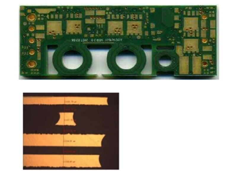
After the etching process, the PCB copper left around a drilled hole is called annular ring. The drilling machine has a tolerance; the center of the hole may not be perfect, and the board also shifts during lamination. When the ring is too small, the drill machine can wander outside the pad, and it causes a drill breakout. Now, as a result, the hole may have copper on one side only; it may or may not pass the electrical test, but it will surely fail in the future. Reusing footprints from the library and hand-placed vias without checking the ring size normally results in drill breakout. |
Figure 1: Left: a normal annular ring with enough copper around. Right: the area around annular ring is copper free. |
Do not place vias near the edge of the board.
The PCB board of our design is a part of a plane; in the end, the router cuts the board outline, and if the copper track is near the edge, then the router may damage it.
This exposes the cooper to an environment that might lead to erosion or contact we don’t really want. It can also create a short circuit between the layers, failing the inspection. It may look fine in the design software, but it will fail in fab.
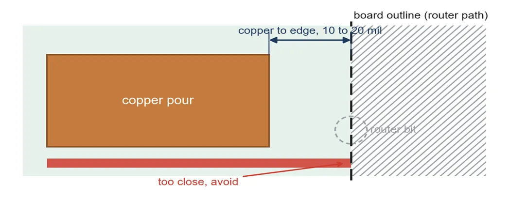
So, it is necessary to keep copper away from the edge. In fab, the traditional safe distance between the edge and copper must be around 10 to 20 mil (0.25–0.5 mm). Always keep the gap according to your related fab guideline.
When two traces in our PCB board meet at a sharp or acute angle, they can make a kind of pocket which traps the etchant for a longer time than normal, which causes it to eat away extra copper at exactly that point. It damages the trace and makes it weak, which can crack under stress.
In modern fabrication houses, current control methods normally eliminate these acid traps, but even then, always route with 45-degree angles instead of sharp corners; it can be considered a tradition and normally can avoid acid traps even if the fab can't eliminate them, and it costs nothing to consider.
Mostly, Design Rule Check (DRC) contains such flags, so turn them on.
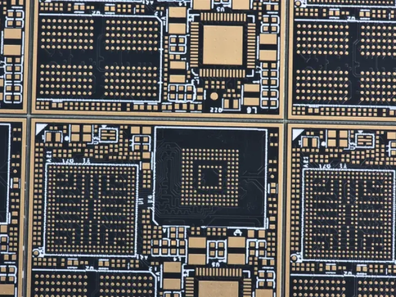
A PCB board where the distance between pads is too small usually has a short film between them called a solder mask. The film or mask should be of suitable length; otherwise, it can’t properly stick.
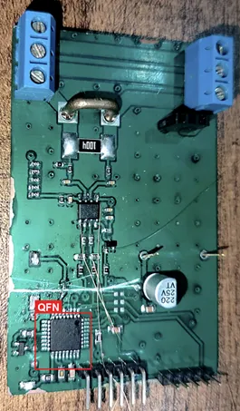
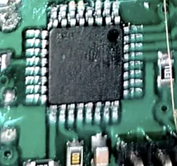
It flakes off during handling, and it leaves pads with no mask between them to keep them separate. QFNs, fine-pitch connectors, and BGAs are usually the reason for the emergence of solder mask failure, where the bridge between pads can't be seen after soldering, and now they are short-circuited.
In an energy monitor plug board shown in Figure 3, the QFN had 5V and ground pins were short circuited with no solder mask dam between them, and the stencil dropped too much paste on the thermal pad.
|
To avoid this, check the flag in DRC for minimum solder mask spacing according to the fab standards.
|
 |
Missing thermal relief on power and ground pours
When a pad is to be connected to a plane with more copper area, like a ground plane, then during soldering, that copper acts as a huge heatsink and heat is sucked away faster than solder ever reaches the proper melting point. So, we get an unreliable joint.

Using thermal relief spokes on pads that connect to planes, which restrict the heat from being sucked away too fast, and create strongly soldered joints.
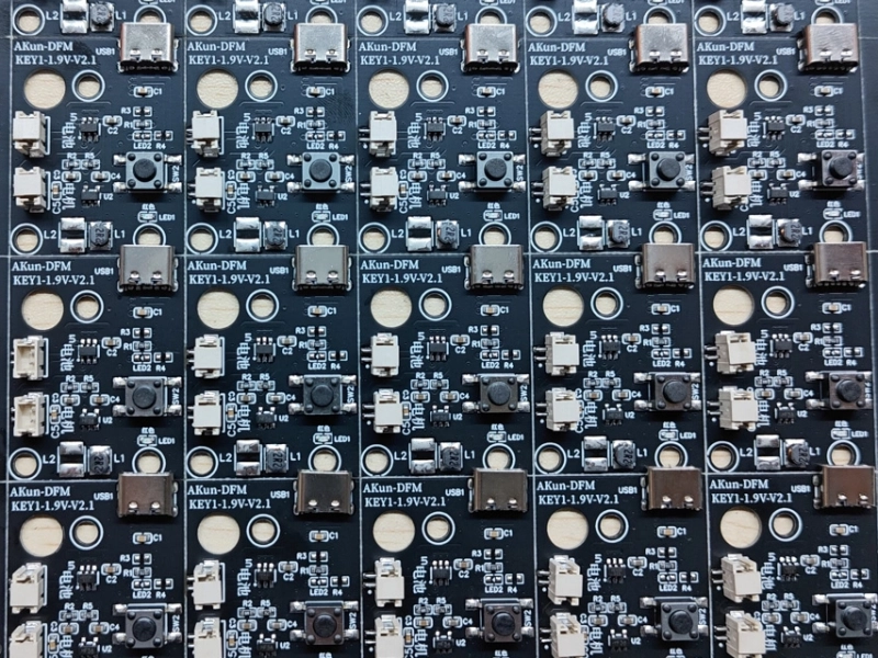
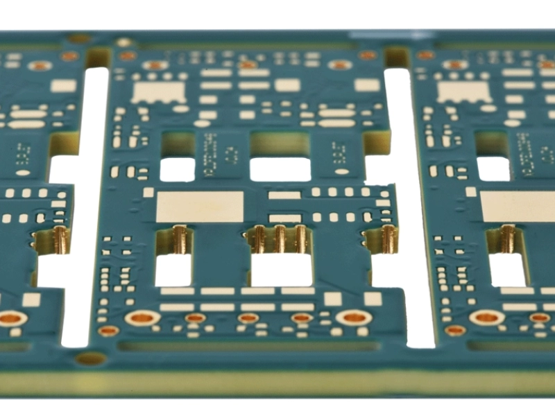
In PCB fabrication, panels and boards are connected using small tabs. If the tabs are not enough, then the panel can break during handling or stress.
And if components with considerable weight are used at the edge of the board, it can also cause the tabs or panel to break. Minimum tab width in fab is about 6 mil (0.15 mm).
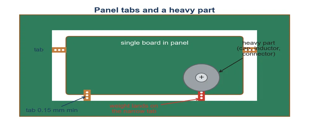
Plan the panelization process with the help of guidelines provided by the fab. Keep the width of the tab according to the related fab standards. Keep heavy components away from the edge of the board.
The solution to these PCB mistakes is simple, and that involves PCB DFM early in the design process.
Most PCB DFM mistakes are due to designing without any fabrication house’s (fab) feedback and then giving files over to fab.
Early collaboration between PCB designers and PCB fab is the key to avoiding these PCB mistakes. First, get the PCB fab’s design guidelines. DRC contains all the flags related to the trace width, annular rings, and others. Check all the flags and remove all the errors. Generate all the required files demanded by fab and send them.
The consequences of these PCB DFM mistakes, rejected boards and fabrication delay, are severe, but they are also avoidable. The right, simple, and early application of PCB Design for Manufacturing (DFM) can improve the chances of getting a working PCB on the first build.
Proven by 7 industries, 4000+ customer projects
|
Please contact us at sales@knownpcb.com, ask for engineering support here or use the form below to reach out to KnownPCB |
Request a Manufacturing QuoteInclude your quantity, target delivery date and key requirements. File handling and NDA information. |