Summary: At KnownPCB, we prioritize "Early-Stage DFM Collaboration" on 8-layer designs, by sharing our 8-layer PCB manufacturing insights, to bridge the gap between design and mass production. This article explains how application requirements affect 8 layer PCB stackup design, including stackup, material selection, manufacturing limits, lamination, drilling and plating, etching, surface finish, impedance control, and production documentation.
1. What Is My Product Application and How to Focus on 8 Layer PCB Stackup Design?
Different industrial applications have very different requirements for PCBs. Not all 8-layer PCBs are the same. The application is what truly determines the stackup, materials, manufacturing process, and cost.
The following scenarios can be used as a reference:
| Application | Typical Products | Key Requirements | KnownPCB Focus |
|---|---|---|---|
| High-speed digital | Servers, FPGAs, communication equipment | Impedance control, low crosstalk, stable return path | Lamination structure, dielectric thickness, impedance tolerance, copper thickness control |
| Automotive electronics | ADAS, BMS, ECU | Reliability, thermal cycling, vibration resistance | Tg, CTE, IPC class, via copper reliability |
| Medical electronics | Portable monitors, implant-related peripherals, imaging equipment | Stability, miniaturization, low noise | Cleanliness, material consistency, traceability |
| Industrial control | PLCs, motor drives, power control systems | High current, interference resistance, environmental durability | Copper thickness, creepage distance, heat dissipation, EMI control |
| Consumer electronics | Mobile phones, wearables, drones | Thin profile, compact size, rigid-flex design | HDI, thin boards, rigid-flex, bending areas |
| RF / wireless | Radar, antennas, communication modules | Low loss, stable phase performance | High-frequency materials, Dk/Df, copper roughness, impedance consistency |
| Power electronics | DC-DC converters, battery packs, inverters | High current, heat dissipation, low voltage drop | Heavy copper, thermal vias, copper balance, warpage control |
Even with the same 8-layer structure, different applications can lead to different materials, stackups, copper thicknesses, via structures, impedance requirements, and testing requirements.
Application requirements define the design goals, but PCB design is not unlimited. It is constrained by manufacturing capability, material properties, reliability, and cost.
2. What PCB Limitations Can Affect Your Design?
2.1 Layer Count Limitations
PCB layout designers often ask:
- Can I use a 6-layer board instead of an 8-layer board?
- Is 8 layers enough, or do I need 10 layers or HDI?
Use the following points as a reference:
| Design Requirement | Possible Limitation | KnownPCB Suggestion |
|---|---|---|
| Multiple high-speed interfaces | Not enough signal layers; return path may be discontinuous | Use a complete GND plane; upgrade to 8 or 10 layers if needed |
| Small BGA pitch | Fanout is difficult; through holes take up too much space | Consider blind vias, microvias, or HDI |
| Complex power network | Too many power plane splits may interrupt the return path | Use a dedicated power plane or local copper areas with proper decoupling |
| High EMI requirements | Signal layers may lack proper reference planes | Place high-speed layers next to solid ground planes |
| Small board size | Routing density may be too high | Evaluate trace width, spacing, and via capability early |
2.2 Impedance Limitations
For example, a PCB designer may request 50Ω, 90Ω, or 100Ω impedance.
KnownPCB recommends understanding that impedance is not a standalone parameter. It is determined by several factors:
- Material Dk
- Dielectric thickness
- Copper thickness
- Trace width
- Trace spacing
- Solder mask thickness
- Inner or outer layer position
- Copper roughness
- Etching compensation capability
- Actual thickness tolerance after lamination
If the PCB designer only provides the target impedance without a stackup, we can help calculate the trace width and spacing. If the layout is already completed, the actual trace width and spacing must be checked to confirm whether the target impedance can be achieved with the selected material and stackup.
2.3 Via Structure Limitations
| Design Choice | Manufacturing Limitation | Risk |
|---|---|---|
| Mechanical through hole | Takes up space across all layers | Routing becomes difficult on high-density boards |
| Blind via | Requires laser drilling and additional lamination processes | Higher cost; reliability needs to be evaluated |
| Buried via | Requires multiple lamination cycles | Longer lead time and higher yield pressure |
| Microvia | Requires tight control of dielectric thickness and copper filling | Via reliability and stacked-via risks |
| Back drilling | Adds extra processing steps | Stub length must be controlled |
BGA pitch, signal speed, board thickness, and via structure together determine whether HDI is needed. It is not decided by layer count alone.
2.4 Copper Thickness, Trace Width, and Spacing Limitations
Many customers have the following PCB layout requirements, but these requirements often conflict with each other:
- High current
- Fine trace width
- Small spacing
- Heavy copper
- High density
Why do these requirements conflict?
| Customer Requirement | Conflict |
|---|---|
| Heavy copper for high current | Etching becomes more difficult, and minimum trace width and spacing increase |
| Fine traces for high-density routing | Not suitable for very thick copper |
| Small board with high power | Heat dissipation may be insufficient, causing local temperature rise |
| Multilayer heavy copper | Higher risk of resin filling issues, warpage, and copper imbalance |
PCB design should not only pursue “finer traces” or “thicker copper.” It must balance current capacity, heat dissipation, impedance, routing density, and manufacturing yield.
These design limitations directly affect the choice of manufacturing process.
3. How Design Parameters Affect the Manufacturing Process
3.1 Material Selection
Material selection should be based on the application:
| Application Requirement | Material Selection |
|---|---|
| Standard digital boards | FR-4 Tg130 / Tg150 / Tg170 |
| High-speed communication | Low-Dk / low-Df materials |
| High-frequency RF | Rogers, PTFE, or hybrid materials |
| Automotive / industrial | High-Tg, high-reliability FR-4 |
| Rigid-flex design | FR-4 + PI flexible core |
| High power | Heavy copper, high-thermal-conductivity materials, metal-core or hybrid structures |
For reference:
- Dk affects impedance and signal delay
- Df affects high-speed signal loss
- Tg affects heat resistance and reliability
- CTE affects via copper fatigue and interlayer reliability
- Copper foil type affects bending life and high-frequency loss
3.2 Lamination Process
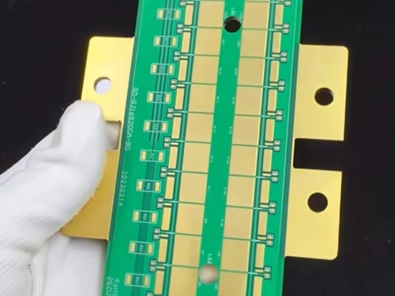
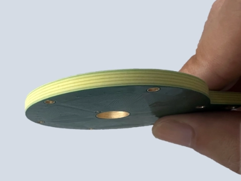
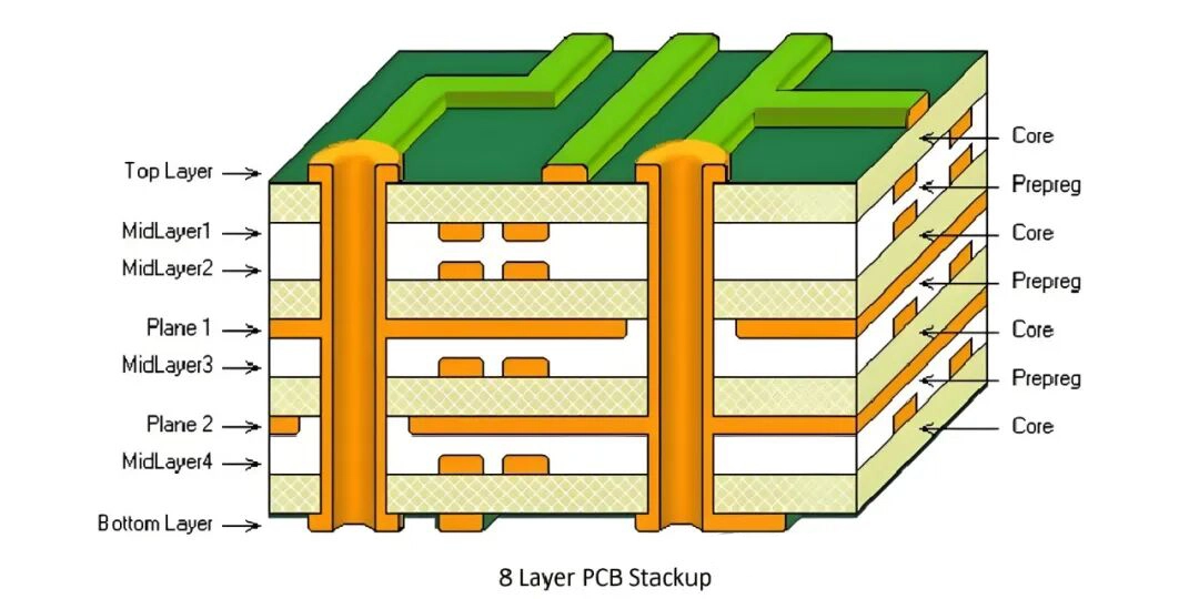
For 8-layer PCBs, the lamination structure directly affects printed circuit board thickness, impedance, warpage, via reliability, and manufacturing yield. Therefore, confirming the stackup early in the design stage is more effective than modifying it after layout is completed.
The key point of an 8-layer PCB is not simply “having 8 layers,” but:
- Which layers are cores
- Which layers are prepregs
- How copper thickness is distributed
- Whether the structure is symmetrical
- Whether heavy copper and thin dielectric are combined
- Whether multiple lamination cycles are required
- Whether blind or buried vias are used
A stackup table from the perspective of an 8-layer PCB manufacturer:
| Layer | Function | Copper Thickness | Reference Layer | Manufacturing Focus |
|---|---|---|---|---|
| L1 | High-speed signal / component side | 1 oz | L2 GND | Outer-layer impedance is affected by solder mask |
| L2 | GND | 1 oz | - | Keep it solid to reduce return path interruptions |
| L3 | Signal | 0.5 / 1 oz | L2 / L4 | Inner-layer impedance is relatively stable |
| L4 | Power | 1 oz | L5 | Pay attention to split planes |
| L5 | GND | 1 oz | L4 / L6 | Provides return path and shielding |
| L6 | Signal | 0.5 / 1 oz | L5 / L7 | Control crosstalk |
| L7 | GND / Power | 1 oz | - | Maintain plane integrity |
| L8 | Low-speed signal / solder side | 1 oz | L7 | Outer-layer etching compensation |
3.3 Drilling and Plating
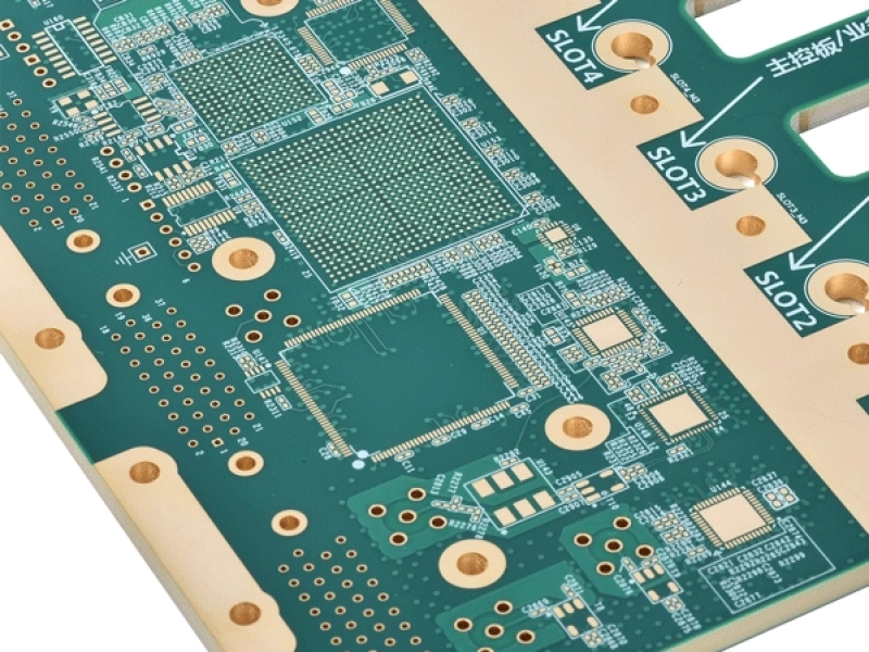
Common PCB design choices affect the manufacturing process. Each added via structure of 8-layer PCB can affect cost, lead time, and reliability.
| Design Action | Impact on Manufacturing |
|---|---|
| Small hole diameter | Increases drilling and plating difficulty |
| High board thickness-to-hole diameter ratio | Reduces via copper uniformity |
| Blind vias | Require laser drilling and via filling |
| Buried vias | Require inner-layer drilling, plating, and then lamination |
| Back drilling | Requires drilling depth control and additional inspection |
| Via-in-pad | Usually requires resin plugging, copper filling, and planarization |
KnownPCB emphasizes:
For high-speed boards, vias are not only connection points but also signal discontinuities. For a PCB manufacturer, vias are key control points for via copper reliability, plating uniformity, and yield.
3.4 Pattern Transfer and Etching
This section is closely related to trace width, spacing, copper thickness, and impedance.
| Design Parameter | Process Impact |
|---|---|
| Finer trace width | Narrows the exposure, development, and etching process window |
| Thicker copper | Increases side etching and makes fine traces harder to control |
| Impedance traces | Require etching compensation and process control |
| Differential pairs | Require tighter control of trace width and spacing consistency |
| Large copper areas | Require copper balance to avoid warpage and uneven plating |
KnownPCB’s summary:
For 8-layer PCB impedance-controlled boards, the final impedance depends not only on the designed trace width but also on the actual trace width after etching. Therefore, KnownPCB usually applies engineering compensation based on the material, copper thickness, and target impedance.
3.5 Surface Finish of 8-layer PCB
PCB surface finish of 8-layer PCB should be selected based on the industrial application, rather than listed as an isolated process choice.
| Surface Finish | Suitable Applications | Notes |
|---|---|---|
| HASL | Standard low-cost boards | Average flatness; not suitable for fine pitch |
| Lead-free HASL | Standard lead-free requirements | Higher thermal shock |
| ENIG | BGA, fine pitch, long-term storage | Higher cost; black pad risk must be controlled |
| OSP | High-volume SMT production | Sensitive to storage time and assembly window |
| Immersion Silver | Some high-frequency / high-speed applications | Sensitive to environmental conditions |
| Immersion Tin | Press-fit or specific soldering applications | Storage and whisker risks should be considered |
| Hard Gold | Gold fingers and plug-in contacts | High cost; usually used selectively |
KnownPCB recommends:
If the PCB layout has BGA, fine-pitch components, or high-reliability requirements, ENIG is usually more suitable than HASL. For cost-sensitive, high-volume SMT production, OSP may be a better option.
4. Impedance Control and Testing
Impedance control and testing for 8-layer PCB are key steps for KnownPCB.
4.1 Basic Process
- The customer provides the target impedance.
- The manufacturer calculates trace width and spacing based on the material and stackup.
- The customer confirms the stackup and impedance table.
- Impedance test coupons are made during production.
- TDR testing is performed.
- An impedance test report is issued.
Impedance control of 8-layer PCB is not something checked only after production. It must be managed throughout stackup design, engineering compensation, pattern imaging, lamination control, and TDR testing.
Reference table:
| Item | Customer Provides | Manufacturer Controls |
|---|---|---|
| Single-ended impedance | Target value, such as 50Ω | Trace width, dielectric thickness, copper thickness |
| Differential impedance | Target value, such as 90Ω / 100Ω | Trace width, spacing, reference layer |
| Tolerance | ±10% or tighter | Material, etching, lamination tolerance |
| Testing method | Whether a report is required | Coupon + TDR |
5. Key Considerations for 8-Layer PCB Design and Production
5.1 Early Design Considerations
Customers should confirm the following before schematic design or layout:
- Whether the layer count is sufficient
- Whether the BGA can be fanned out
- Whether blind vias or buried vias are required
- Whether impedance control is required
- Whether there are high-current areas
- Whether there are high-temperature components
- Whether there are bending areas
- Whether special certifications are required
- Whether special materials are required
- Whether IPC Class 3 is required
KnownPCB emphasizes:
The later the stackup is confirmed, the higher the modification cost. For high-speed boards, HDI boards, and rigid-flex boards, the stackup and impedance plan should be confirmed before layout.
5.2 8-Layer PCB Layout Considerations
- High-speed signals should have a continuous reference plane.
- Do not route high-speed signals across split planes.
- Keep differential pair trace width and spacing consistent.
- Control the number of vias and stubs.
- Place decoupling capacitors close to power pins.
- Consider copper width and heat dissipation for high-current paths.
- Maintain copper balance on large copper areas.
- Keep high-speed traces away from the board edge.
- Avoid vias and pads in rigid-flex bending areas.
- Confirm the BGA fanout plan in advance.
5.3 Gerber and Production File Considerations
KnownPCB shares the following checklist for placing a PCB order:
| File / Information | Why It Matters |
|---|---|
| Gerber or ODB++ | Basic production data |
| NC Drill | Drilling data |
| Stackup drawing | Confirms layer order, materials, and thickness |
| Impedance table | Defines impedance control requirements |
| Fab notes | Defines process requirements and acceptance criteria |
| IPC Class | Determines acceptance standards |
| Surface finish | Affects solderability and reliability |
| Copper thickness | Affects current capacity, impedance, and etching |
| Solder mask color | Affects appearance and some inspection steps |
| UL / RoHS / REACH requirements | Affects material selection and certification |
| Panelization requirements | Affects assembly and cost |
If you are unsure about the stackup, impedance, or process parameters, they can send the schematic, key component packages, and interface speeds to the PCB manufacturer before layout for DFM and stackup pre-evaluation.
Need 8-Layer PCB Stackup or DFM Pre-Evaluation?
If you are unsure about the stackup, impedance, or process parameters, you can send the schematic, key component packages, and interface speeds to KnownPCB before layout for DFM and stackup pre-evaluation.