In PCB fabrication, PCB panelization is a silver bullet for maximization of efficiency, whether for PCB prototyping or low-volume orders. The priority solution for PCB array design is panelization to optimise PCB space.
It is not a black and white answer.
In the environment of PCB prototyping or low volume, PCB panelization is deceptively simple at first glance, but in practice, a strategic trade-off between PCB fabrication processing and cost.
A smart PCB array design can further slash the cost, but an unreasonable solution often backfires in the long run.
KnownPCB explored the nuances of the “cost-invalidation” in PCB panelization.
Let’s take a closer look at the the types of PCB panelization offering a good value and which ones to avoid.
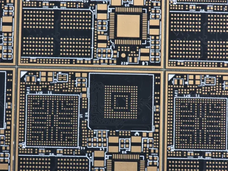
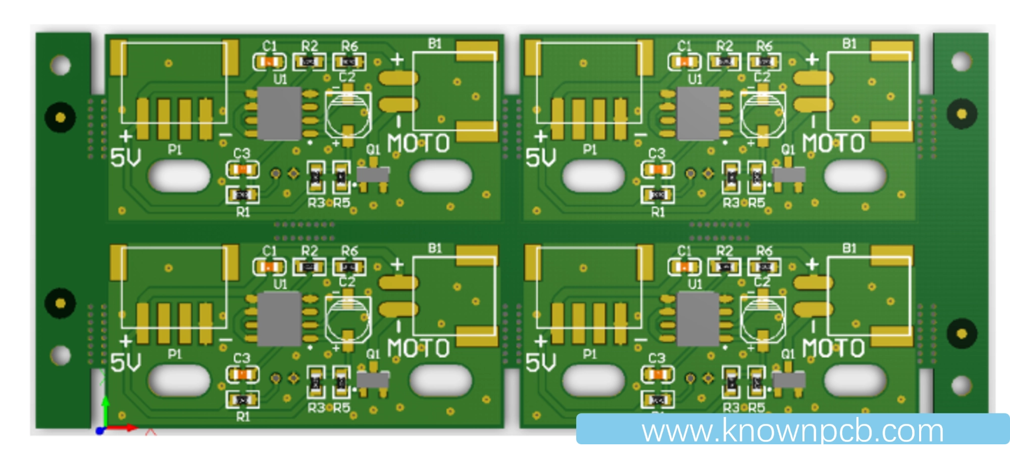
Known as panelizaiton, this method of grouping multiple small blank PCBs into a single and large PCB sheet. The completed PCB will be separated to individual units. The common approaches of panelization are uniform array, family nesting (dissimilar designs), rotating boards. The design consideration factors are taken into PCB panelizaiton solution. 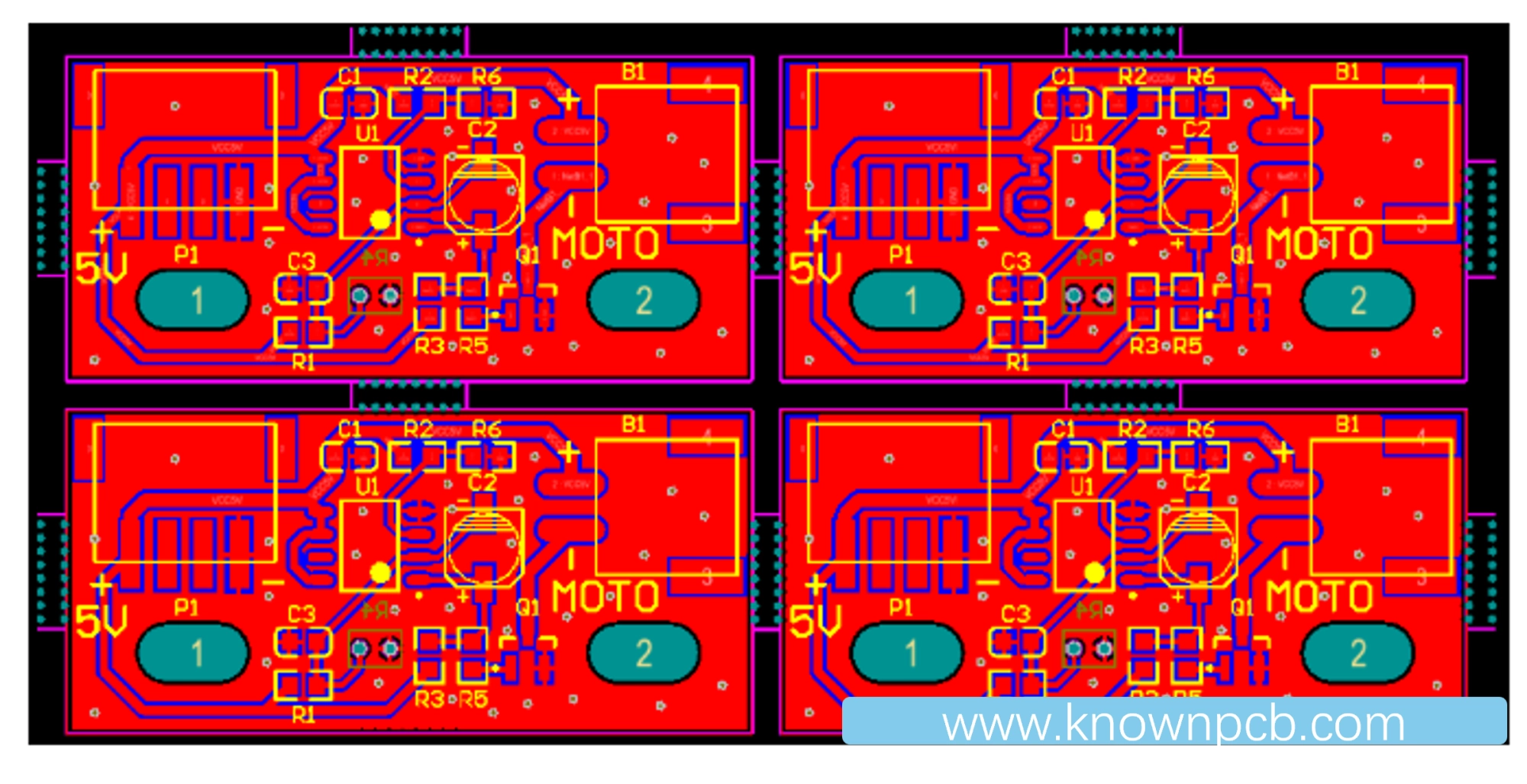
KnownPCB team has listed the definite advantages of PCB panelization.
A key lever for PCB manufacturing cost, PCB panelization is driving the material utilization and amortizing fixed costs. Especially during the NPI stage, it creates obvious benefits for low-volume or prototyping PCB requirements.
Uniform PCB panels with larger size reduce indexing frequency during SMT processing and significantly enhance production throughput.
Panelization manufacturing not only simplifies pick-and-pack operations, but also provides more robust protection and reduces shrinkage.
But PCB designers are often blind-sided by the hidden traps of PCB panelization.
The non-standard shaped PCBs mounts the challenge for time-consuming in handling manual layout that led an overhead cost.
KnownPCB has moved beyond a simple DFM software, we identify the most effective orientation of irregular-shape PCB designs by smarter modern DFM tools.
Of cause, it is hard for hardware or PCB designers to balance the number of panelization and manufacturing constraints.
The desire of “more is cheaper” caused over panelization during the low-volume PCB or prototyping phase.
The second pitfall, in practice, will result in a series of manufacturing risks, for example, placement deviation, PCB board warpage and sagging.
As a PCB manufacturer since 2008, KnownPCB team provides clear and strong engineering intervention instead of “only-print” service at a rapid-response feedback loop.
The tech guides include mandatory dimensional control, A/B flip panel, prohibiting V-scoring for overhanging components, complimentary CAM reviews and specialized engineering support for High-Frequency (HF) applications.
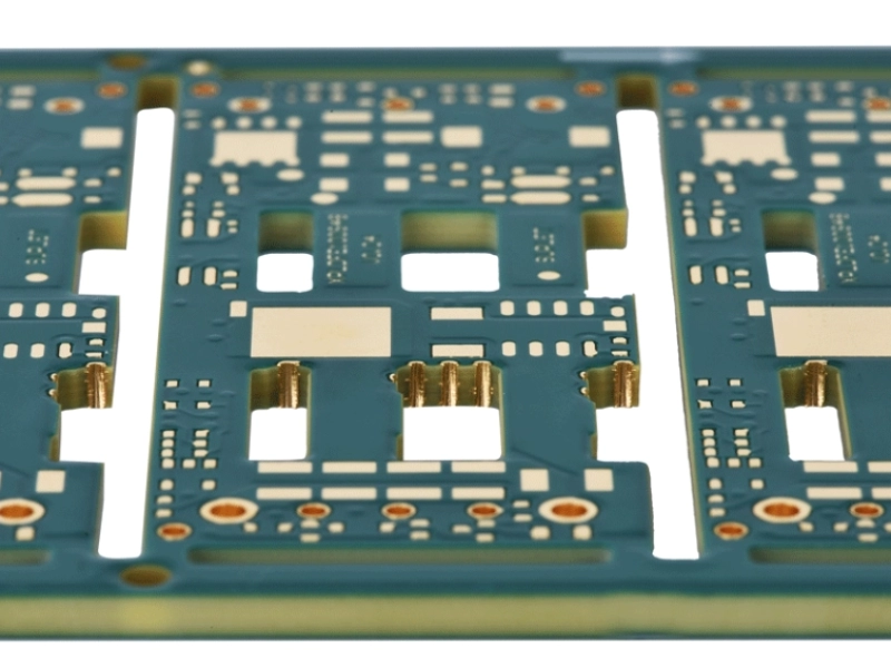
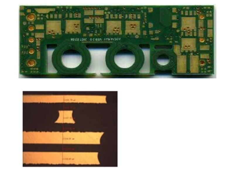
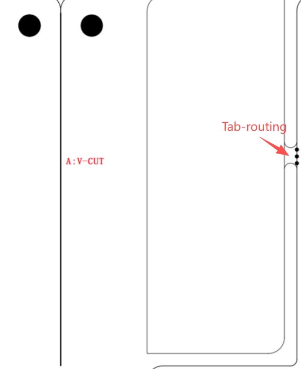
The type of PCB panelization can be involved in v-scoring, tab-routing, or CNC routing. However the PCB may end up as scrap if no clear depanelization methods.
Here are some common design errors and solutions as a reference for cost & timing-saving PCB panelization.
V-scoring is applied into regular-shape design. PCB design note: keep linear and perfect alignment.
Tab-routing in PCB panelized is a recommendation for irregular-shape design. PCB design note: classic range of hole dimension is from 0.3mm to 0.5mm and a pitch of 0.4-0.6mm. It will be easier to panelize.
KnownPCB will give advice for the PCB panelization and depanelization method before prototyping or low-volume fabrication.
Ensuring every dollar contributes to a high-yield, high-reliability outcome of your PCB project.
Request for a tech support
 | Download our design guidesfor better PCB designing and manufacturing These are some of the design guides designers and engineersdownload the most:
|
Proven by 7 industries, 4000+ customer projects
Please contact us at sales@knownpcb.com, ask for engineering support here or use the form below to reach out to KnownPCB | Get In Touch Today |