KnownPCB, a China-based PCB manufacturer, is always trying to make PCB perfect.
But PCB surface defect is an insidious of PCB quality issues.
It is about localized separation of the copper layer from the substrate.
On paper, the factors of PCB surface defect are simple sentences. But it’s a different story in the real world of manufacturing.
Started with a definition of the defect: During electroless copper deposition or electroplating in the PCB manufacturing process, unstable surface preparation or bath chemistry undermines interfacial adhesion.
The incorrect processing of etching in PCB processing, no matter over-etching or under-etching, breaks down the foundation of trace.
What happens when the etching process leaves behind more—or less—than it should?
•Adhesion failure, eg. the insufficient gold thickness cause wear-through to the nickel underplate after 500 cycles of repeated mating cycles.
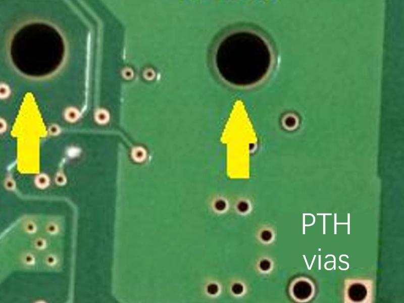
•Barrel cracking acts as a role of latent risk, it passes initial testing but fails later due to mismatched CT. As the PTH of PCB suffers strong piston, it is typically failure at operating heat.
•Disable CAF: The areas of insufficient under-etch lead to electrochemical migration, the chip burns out in high-humidity environments.
•Poor Wetting: The solder curled up into a stubborn, 'bulbous' dome. This is the root cause of non-wetting, leading to an 18% pseudo-soldering rate.
Inner layers of PCB must undergo a desiccation baking at pre-lamination to achieve a sufficient dryness and reduce the risk of blistering and barrel cracking.
It is a definitive way to inspect strictly thermal profiling and Tg verification during PCB fabrication.
Once the pressing is done, we don't just stop there. We take those semi-finished PCB boards and post-bake into the oven at 140°C for another 2 to 6 hours. This 'post-bake' is what really locks in the final cure during the PCB process.
Aside from strict process control of chemical oxide bath, which is essential, a more tangible intervention-such as the inspection of PCB surface in KnownPCB. Complementing the measures with Double-Treated Foil(DTF) provides a more robust guard. This is a part of KnownPCB quality guarantee system.
We have found that the most challengeable operation management during PCB manufacturing is the sources of contamination that people carry dust during routine actions. KnownPCB sets a rigorous standard about the defense of “carry-overs”.
1.Frequently strengthen cleanliness management;
2.Minimize direct hand contact and repeated panel picking;
3.Properly covered to the material;
4.Strictly separated the operation area of tooling maintenance and registration.
KnownPCB production manager, Ms Jiang shared PCB knowledge about lamination pressure and routing inspection:
1.Proper length of pins keeps away bottoming out with over-extension.
2.Flatness of separator plates
3.A perfect situation of vacuum seal system
4.Micro-adjustment on Pressure: slightly boost lamination pressure to improve compaction.
5.Fine-tune or scale back the applied lamination pressure as needed.
Ms Wu, the manager of quality management from KnownPCB told us, " We incrementally scale our lamination pressure to ensure the assembly can endure five 288°C/10-second solder float cycles, serving as a validation of peak interfacial bond strength."
Rather than being static mandates, these operation guideline about PCB surface quality management represents a self-correcting process loop distilled from extensive mass production experience in KnownPCB manufacturing.
Empowering 4,000+ customers across the globe with specilized PCB manufacturing, rapid prototyping, High-Mix Low-Volume (HMLV), assembly.
Learn more about service details, 1-Hour instant quotation, free DFM at www.knownpcb.com
Request for a tech support
 | Download our design guidesfor better PCB designing and manufacturing These are some of the design guides designers and engineersdownload the most:
|
Proven by 7 industries, 4000+ customer projects
Please contact us at sales@knownpcb.com, ask for engineering support here or use the form below to reach out to KnownPCB | Get In Touch Today |