HASL(Hot Air Solder Leveling) · Most common · low cost · Limited flatness · Thickness: 1-40 μm | ENIG(Electroless Nickel Immersion Gold) · Flat surface · Good solderability · Nickel (Ni): 3-5 μm · Gold (Au): 0.25-1.27 μm | Hard Gold(Electroplated Hard Gold) · Excellent contact reliability · High wear resistance · Gold (Au): 0.025-0.127 μm · Nickel (Ni): 3-5 μm |
 |  |  |
| Characteristic | HASL | ENIG | Notes |
|---|---|---|---|
| Cost | Low | High | ENIG requires expensive nickel and gold chemicals; HASL is the most cost-effective option. |
| Surface Flatness | Poor | Excellent | HASL pads have solder domes (not flat); ENIG produces very flat and uniform surfaces. |
| Solderability | Excellent | Good | HASL provides a pure tin surface (excellent for soldering); ENIG’s nickel layer is solderable but inferior to pure tin. |
| Shelf Life / Oxidation Resistance | 12 Months | 6 Months | HASL can still solder well after long storage; ENIG surfaces are stable but sometimes specified with shorter shelf life. |
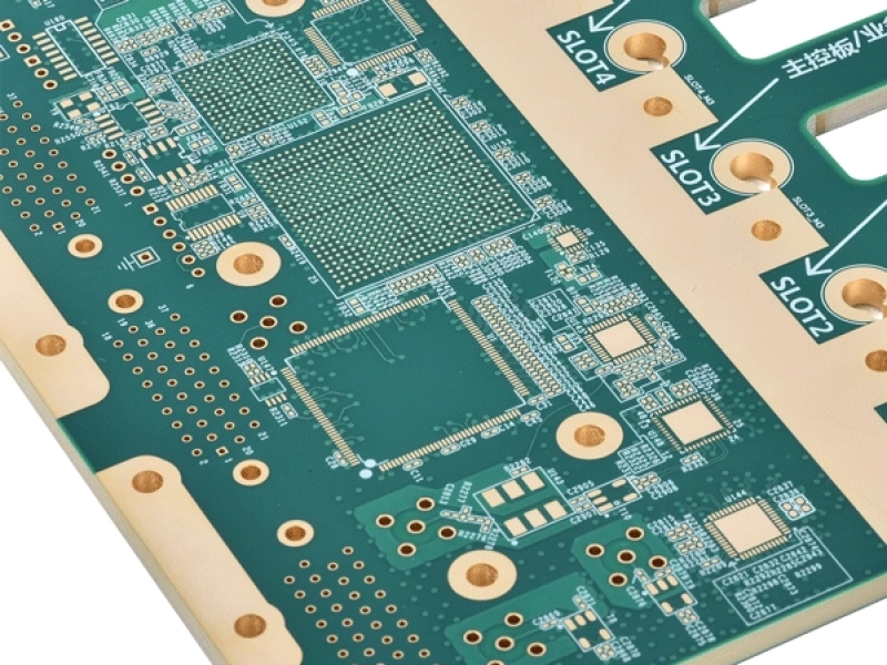
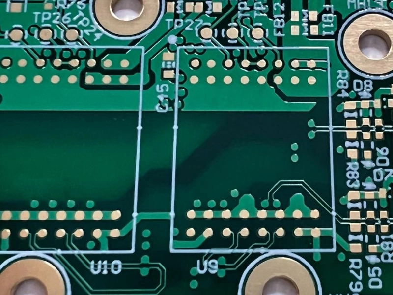
| Suitable Components | Large-pitch components | Fine-pitch components (BGA, QFP, etc.) | Uneven HASL may cause bridging in fine-pitch parts; ENIG flatness is essential for BGA and fine-pitch SMT. |
| Environmental Compliance | Leaded HASL is non-RoHS; lead-free HASL is RoHS-compliant | RoHS-compliant | ENIG contains no lead and fully meets RoHS. Modern HASL is usually lead-free. |
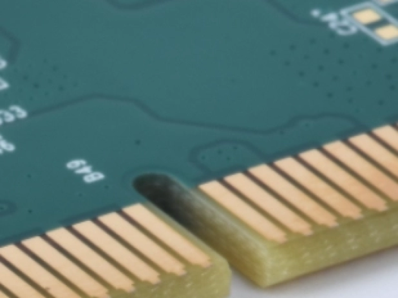
| Additional Applications | Soldering only | Also for contact surfaces (e.g., gold fingers, keypads) | ENIG’s gold layer is durable and conductive, suitable as a contact surface. |
| Process Risks | Thermal stress may cause board warpage | “Black pad” risk | HASL uses high temperature and may warp boards; ENIG can suffer nickel corrosion if process control fails. |
| Appearance | Bright silver (leaded) or matte silver (lead-free) | Gold color, aesthetically pleasing | HASL is rough-looking; ENIG is smooth and visually attractive. |
| Characteristic | ENIG | Hard Gold Board | Notes |
|---|---|---|---|
| Process Principle | Chemical displacement plating | Electroplating (requires external current) | ENIG is purely chemical; hard gold requires current and plating connections. |
| Gold Type | Pure gold (soft gold) | Gold-cobalt or gold-nickel alloy (hard gold) | Soft gold is ductile; hard gold is wear-resistant. |
| Gold Thickness | Thin, typically 0.025–0.127 μm | Thick, typically 0.25–1.27 μm or more | ENIG uses very thin gold for solderability; hard gold has a thick layer for durability. |
| Nickel Thickness | 3–5 μm | 3–5 μm (as base layer) | Both require nickel as a diffusion barrier. |
| Surface Flatness | Excellent, very flat, suitable for SMT fine-pitch | Moderate, may show edge effect | ENIG ensures flatness; electroplating can cause non-uniform edges. |
| Wear Resistance | Poor, soft gold is easily scratched | Excellent, very durable | Hard gold is highly resistant to insertion/removal cycles. |
| Solderability | Excellent, pure gold has slow oxidation | Poor, alloy gold oxidizes and is not recommended for soldering | ENIG for soldering, hard gold for wear resistance. |
| Cost | Lower, simpler process, economical for mass production | Higher, requires electroplating steps, more gold consumption | Hard gold plating is costly due to extra process and thicker gold. |
| Applications | Mainstream: SMT, BGA, fine-pitch packages in consumer electronics, telecom, etc. | Special use: edge connectors, gold fingers, test pads, frequent contact areas | ENIG for soldering; hard gold for wear areas. |
| Design Considerations | No special layout requirement, can cover full PCB | Requires plating traces (thieving lines), increases layout complexity | Hard gold requires specific PCB design features for plating. |
| Common Issues | Black pad: nickel layer corrosion leads to brittle solder joints | Uneven thickness: thicker at edges, thinner in the middle | Process control is critical for both. |
Request for a tech support
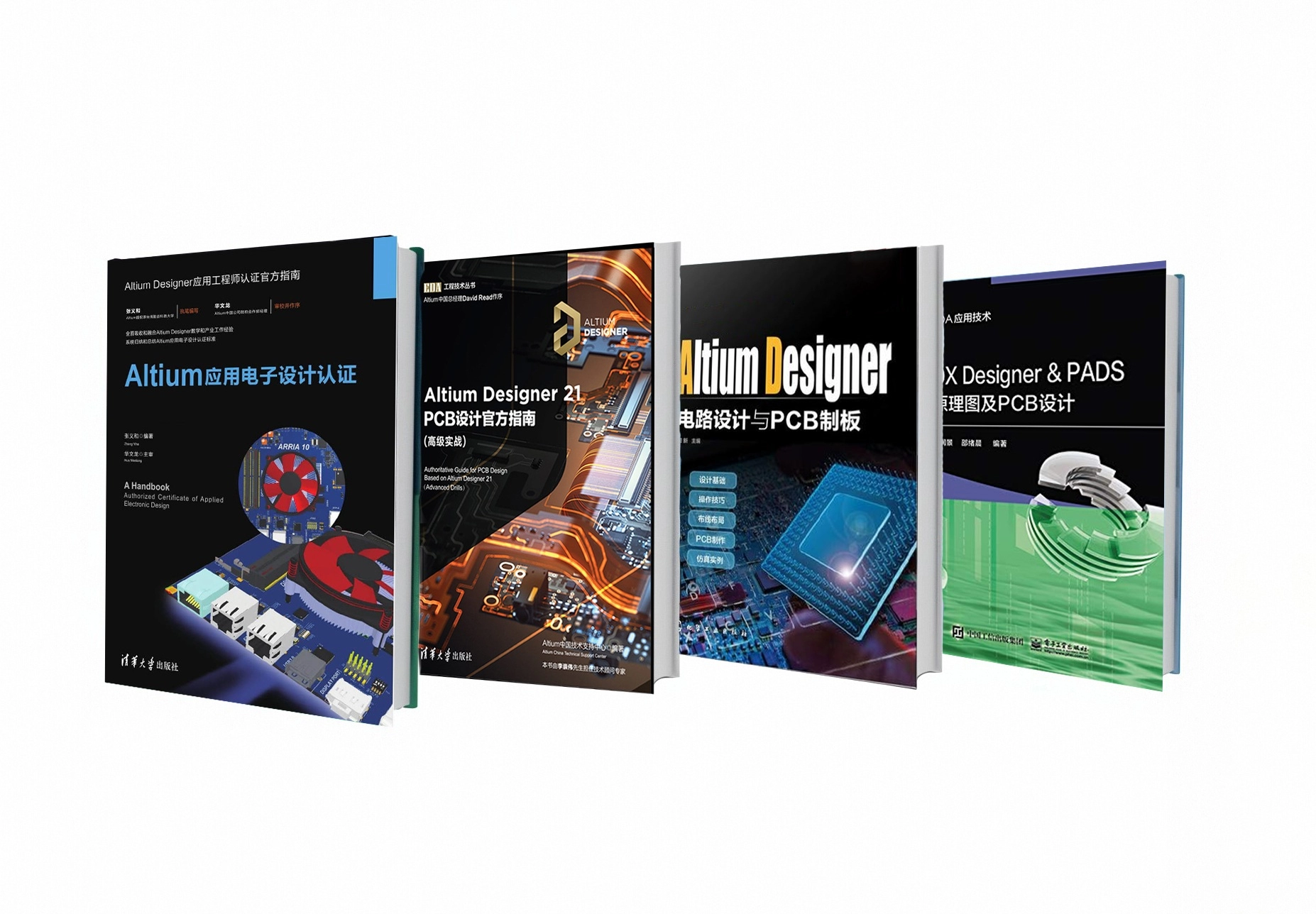 | Download our design guidesfor better PCB designing and manufacturing These are some of the design guides designers and engineersdownload the most:
|
Proven by 7 industries, 4000+ customer projects
Please contact us at sales@knownpcb.com, ask for engineering support here or use the form below to reach out to KnownPCB | Get In Touch Today |