Understanding the difference between impedance-designed, controlled impedance, and verified impedance helps determine whether controlled-impedance PCB manufacturing is necessary for your project. You've designed your PCB using the right choice of materials and followed the required procedures, only to find your signal distorted or data corrupted. When this happens, designers may first suspect the components and attempt to replace them.
However, the actual problem may be something less obvious: the impedance is not being adequately controlled.
Controlled impedance was once commonly associated with specialized RF boards. Today, decreasing rise times, increasing data rates, and mixed-signal designs mean that predictable transmission-line behavior has become important for many modern PCB projects.
The key manufacturing question is not simply what impedance your calculator predicts. It is whether the fabricated PCB can consistently deliver the intended impedance within a usable tolerance after real material, etching, plating, lamination, and copper-thickness variations are taken into account.
What Is a Controlled Impedance PCB and When Is It Needed?
A controlled-impedance PCB is a board in which the characteristic impedance of selected single-ended or differential traces is deliberately managed through material selection, stackup design, trace geometry, and manufacturing process control. The objective is to ensure that the finished board meets a specified impedance target and tolerance.
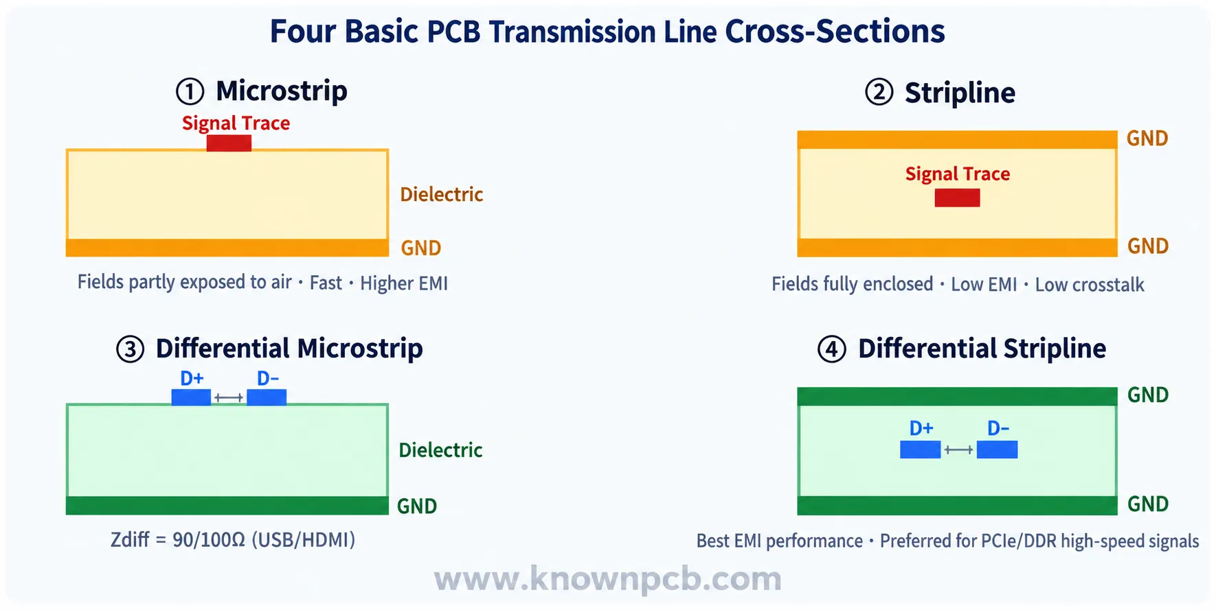
Controlled impedance becomes increasingly important when the electrical length of a trace is significant relative to signal rise time and transmission-line effects such as reflections, distortion, or loss of signal integrity can affect system performance.
Typical Interface Impedance Reference Parameters
| Application / Interface | Typical Reference | Example Tolerance | Design Focus |
|---|---|---|---|
| RF Transmission Line | 50 Ω single-ended is common | Project dependent | Low-loss material, reference plane, transitions and connector launch |
| USB | 90 Ω differential | Example guidance: ±15% | Pair geometry, return path, symmetry and via transitions |
| HDMI TMDS | 100 Ω differential | Example guidance: ±15% | Differential geometry, pair matching and impedance discontinuities |
| PCI Express | 85 Ω differential in representative motherboard guidance | Example guidance: ±15% | Pair matching, reference plane, vias and topology |
| Ethernet PHY | 100 Ω differential | Example device guidance: ±5% | Pair symmetry, ground reference, spacing and minimal via use |
Engineering note: These figures are reference parameters rather than universal fabrication specifications. Always confirm the applicable interface specification, device vendor guidance, stackup, and PCB manufacturer's process capability before releasing production data.
How to Decide Whether Controlled Impedance Is Needed
| Factor | Lower-Risk Condition | Higher-Risk Condition | Implication |
|---|---|---|---|
| Signal rise time | Slow edge | Fast edge | Faster edges increase transmission-line sensitivity |
| Critical trace length | Electrically short | Electrically long relative to rise time | Longer electrical paths increase reflection risk |
| Interface specification | No defined impedance requirement | Defined target and tolerance | Specified interfaces normally require controlled routing |
| Return path | Continuous reference plane | Plane splits or multiple transitions | Discontinuities increase impedance and EMI risk |
| Performance consequence | Large variation is acceptable | Failure affects timing, RF performance or compliance | Higher consequence supports tighter process control and verification |
A short, low-speed net that can tolerate substantial impedance variation may be adequately manufactured using a standard PCB fabrication process. If transmission-line behavior directly affects performance, as with RF feed lines or tightly timed high-speed buses, controlled impedance becomes much more important.
Impedance-Designed vs Controlled vs Verified
These three terms are sometimes treated as interchangeable, but they represent different levels of manufacturing assurance.
| Level | What It Means | Manufacturer Action | Evidence | Assurance Level |
|---|---|---|---|---|
| Impedance-Designed | Layout and stackup are calculated around a target impedance. | Fabricates according to provided dimensions and stackup assumptions. | Field-solver or formula result. | Basic |
| Controlled Impedance | Manufacturing variables affecting actual impedance are actively controlled. | Confirms stackup, selects materials, manages copper and adjusts artwork using process capability. | Controlled manufacturing process. | Higher |
| Verified Impedance | Finished production is measured against the specified target and tolerance. | Uses test structures such as impedance coupons and measurement equipment such as TDR. | Measured production result / report. | Highest |
Impedance-Designed
An impedance-designed PCB uses a target impedance when determining its layout and stackup, normally with a field solver or approximate formulas. The designer expects the fabricated board to reproduce the calculated structure.
In practice, actual laminates can vary in dielectric constant, resin content, and dielectric thickness. Finished trace geometry can also change because of copper foil profile, etching, plating, and etch undercut. The calculated impedance should therefore be treated as the design starting point rather than proof of the final result.
Controlled Impedance
With controlled impedance manufacturing, the PCB fabricator actively manages variables capable of changing actual impedance. This can include stackup confirmation, material selection, copper-thickness control, dielectric-thickness control, and etch compensation.
The objective is to manufacture boards that remain within the required impedance window in production rather than merely matching a theoretical model.
Verified Impedance
Verified impedance adds measurement to the process. Finished production or representative test coupons are measured to determine whether the combination of design, materials, and manufacturing process actually delivers the specified impedance. Without measurement, neither the designer nor the manufacturer has objective production evidence that the intended electrical target has been achieved.
How to Specify Controlled Impedance Requirements
The PCB manufacturer needs more than a single impedance number. A practical impedance specification should connect each controlled net to its layer, structure, target, tolerance, material system, and verification requirement.
| Parameter | What to Provide | Example |
|---|---|---|
| Net / Class | Controlled trace names or net classes | USB_D_P / USB_D_N |
| Layer | Routing layer for each impedance structure | L1 referenced to L2 GND |
| Type | Single-ended or differential | Differential pair |
| Target | Nominal impedance | 100 Ω differential |
| Tolerance | Acceptable production range | ±10% |
| Material | Preferred / restricted laminate and electrical requirements | Specified laminate family, Dk / Df requirements if applicable |
| Stackup | Copper weight and dielectric thickness | Defined according to approved stackup |
| Geometry Limits | Allowed trace width and pair spacing adjustment | Manufacturer adjustment permitted after engineering review |
| Verification | Coupon and measurement/report requirement | TDR coupon + lot report |
How Controlled Impedance PCBs Are Manufactured
Controlled impedance manufacturing is not a simple build-to-drawing process. Multiple material and process variables must work together to keep the final transmission-line geometry within the intended electrical range.
| Stage | Key Parameters | Why It Matters to Impedance |
|---|---|---|
| 1. Material Selection | Dk, dielectric thickness, thickness tolerance, resin system, copper profile | Changes electromagnetic field distribution and effective impedance |
| 2. Stackup Review | Signal layer, reference plane, dielectric separation and copper weight | Defines the physical transmission-line structure |
| 3. CAM / Etch Compensation | Artwork width, copper weight, etch factor and historical process data | Compensates for width reduction or geometry changes during etching |
| 4. Lamination | Pressure, temperature, time and final dielectric thickness | Dielectric thickness variation directly affects impedance |
| 5. Copper / Plating Control | Base copper, plated copper and thickness distribution | Finished conductor dimensions differ from nominal artwork geometry |
| 6. Verification | Coupon structure, target impedance, tolerance and TDR result | Confirms whether the manufactured structure meets the electrical requirement |
Controlled Impedance PCB Cost: What You Pay For
Controlled impedance can increase PCB manufacturing cost because the job requires additional engineering review, tighter process control, possible material restrictions, and potentially electrical verification. The exact premium depends on the board structure and required tolerance.
| Cost Driver | What Adds Cost | Typical Impact |
|---|---|---|
| Engineering | Stackup review, impedance calculation and CAM compensation | Additional pre-production engineering |
| Material | Higher-performance or tighter-tolerance laminate systems | Higher material cost |
| Verification | Test coupons, TDR measurement and reporting | Additional testing and documentation |
| Tolerance | Narrower permitted production window | More demanding process control and potentially lower yield |
| Production Volume | Engineering and setup costs spread across fewer units | Low-volume jobs may have a higher unit cost |
| Documentation | Lot-level measurement records or additional reports | Additional quality-control workload |
Cost comparison tip: When requesting quotations, do not compare only the final PCB unit price. Confirm whether stackup engineering, impedance coupons, TDR testing, reports, special materials, and tolerance requirements are included in the quotation.
Choosing a Manufacturer and Application Considerations
Not every PCB manufacturer provides the same depth of controlled-impedance capability. The important distinction is whether the supplier can connect design requirements with material control, CAM engineering, production capability, and measurement.
| Capability to Check | What to Ask | Why It Matters |
|---|---|---|
| Stackup Control | Can the factory provide and confirm a production stackup? | Impedance depends on actual dielectric and copper construction |
| Material System | Which FR-4 or high-frequency materials are supported? | Material electrical properties affect the impedance model |
| CAM Engineering | Can trace widths and spacing be adjusted after engineering review? | Production geometry can differ from design geometry |
| Process Capability | How are dielectric thickness, etch factor and copper distribution controlled? | These variables directly affect finished impedance |
| TDR Verification | Are impedance coupons tested and reports available? | Provides objective evidence of production performance |
| DFM Collaboration | Will engineering communicate required stackup or geometry changes before fabrication? | Reduces mismatch between layout assumptions and actual manufacturing capability |
Application-Specific Controlled Impedance Considerations
| PCB / Application Type | Typical Structures / Signals | Parameters Requiring Attention |
|---|---|---|
| RF PCB | 50 Ω transmission lines, microstrip, stripline or coplanar structures | Dk, Df, line width, ground spacing, ground transitions, connector launch and via effects |
| High-Speed Digital PCB | USB, Ethernet, HDMI, PCIe and other serial interfaces | Differential impedance, intra-pair skew, length matching, via transitions and return-path continuity |
| DDR / Memory PCB | Clock, strobe, address, command and data groups | Topology, impedance class, timing matching, reference plane and layer transitions |
| HDI PCB | Fine traces and microvia transitions | Microvia geometry, thin dielectric construction, copper plating and transition discontinuities |
| Flex / Rigid-Flex PCB | Controlled traces crossing rigid and flexible regions | Coverlay effects, dielectric structure, copper type and rigid-to-flex impedance continuity |
Example: Turning a Design Requirement Into Manufacturing Parameters
| Interface | High-speed differential interface |
| Target | Example: 100 Ω differential |
| Tolerance | Specified according to applicable interface / project requirement |
| Reference Structure | Signal layer referenced to a continuous ground plane |
| Geometry | Final trace width and spacing calculated from the approved production stackup |
| Manufacturing Adjustment | CAM compensation based on actual copper, dielectric and etch capability |
| Verification | Representative impedance coupon measured by TDR when required |
Frequently Asked Questions
1. What is the difference between calculated impedance and measured impedance on a finished PCB?
Calculated impedance is a predicted value based on parameters such as dielectric constant, dielectric thickness, copper thickness, trace width, and spacing. Measured impedance is obtained from the actual fabricated PCB or representative test coupon and therefore reflects the combined result of material and manufacturing variation.
2. Do I always need controlled impedance for high-speed digital interfaces such as USB, HDMI, or PCIe?
High-speed interfaces commonly have specified transmission-line requirements, but the engineering significance of impedance control also depends on factors such as signal rise time, route length, topology, return path, and acceptable system margin. Electrically long traces and tightly specified interfaces normally make impedance control much more important.
3. How much does controlled-impedance PCB manufacturing add to the cost?
There is no universal percentage. The additional cost depends on material selection, impedance tolerance, stackup complexity, number of controlled structures, production quantity, testing requirements, and whether TDR reports or other lot-level documentation are required.
Conclusion
Controlled-impedance PCB manufacturing is about turning a theoretical transmission-line target into predictable production performance. Design calculation, material selection, stackup engineering, process control, and measurement each contribute to the final result.
If your next PCB contains controlled nets, impedance should be treated as a manufacturing requirement rather than simply a layout value. Discuss material selection, stackup, trace geometry, allowable CAM adjustments, target tolerance, and verification requirements with your PCB manufacturer before production.
By Amy Jiang,
18-year sale engineering experience in PCB industry. A versatile sales engineer with both engineering background and international project experience. She is familiar with HDI, high-speed boards and small-to-medium batch manufacturing requirements. Being capable of quickly understanding the design pain points of customers and providing a one-stop PCB solution from DFM to mass production.
Need Controlled Impedance PCB Manufacturing?
Known PCB provides PCB manufacturing services including controlled-impedance PCB production. Send us your stackup, impedance requirements, controlled-net information, material requirements, and testing needs so our engineering team can review the manufacturing requirements before production.
Get a Free PCB Quote