By Amy Jiang
18-year sale engineering experience in PCB industry. A versatile sales engineer with both engineering background and international project experience. She is familiar with HDI, high-speed boards and small-to-medium batch manufacturing requirements. Being capable of quickly understanding the design pain points of customers and providing a one-stop PCB solution from DFM to mass production.
Suppose you’re choosing between ENIG and HASL. It comes down to what the PCB must tolerate before as well as during assembly. The higher price of ENIG is okay when
- Small pads need a flat surface.
- Fine-pitch packages complicate solder paste printing.
- Bare boards may wait longer before assembly.
What about HASL or lead-free HASL? It might be the sensible buy for
- Larger-pitch parts.
- Through-hole designs.
- General prototypes.
This is where slight unevenness is allowed and won’t disturb placement.
If we talk in a practical way, the smallest land pattern is a better starting point when it is compared to a blanket shop-floor preference. Moreover, you should keep in mind that neither finish automatically becomes better. Basically, different factors are helpful in deciding which option deserves the purchase order. These factors include but are not limited to component geometry, assembly capability, storage, compliance and first-pass yield.
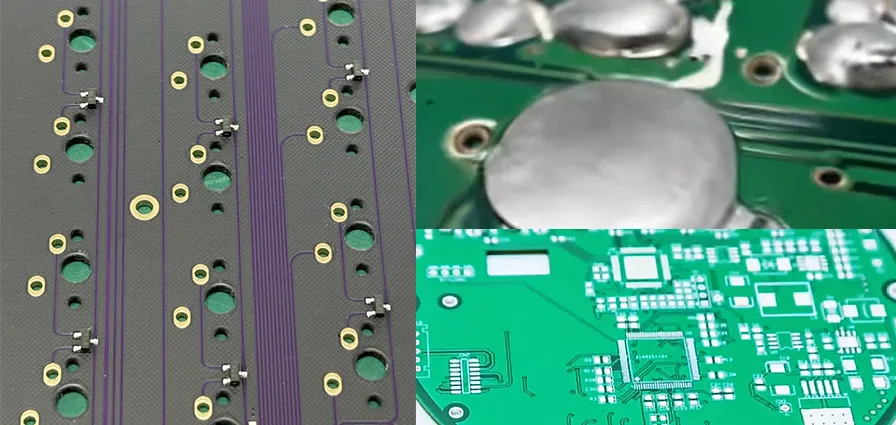
ENIG or HASL. Quick Selection Guide
You can choose ENIG If
- Your layout makes use of BGA, QFN, CSP or other flatness-sensitive packages.
- Fine-pitch pads leave little tolerance for inconsistent solder height.
- Assembly schedule includes delayed builds or several thermal cycles.
- Avoiding paste-printing and coplanarity trouble justifies a costlier finish.
Now let’s come to the other option. You can choose HASL If
- Finish price is a major constraint.
- Components use larger pads or wider pitch.
- Through-hole content outweighs dense SMT placement.
- Board is a straightforward prototype or general-purpose design.
| Factor | ENIG | HASL | Why for Selection |
|---|---|---|---|
| Pad surface | Very flat | More variable | As pitch shrinks, uniform pads are more important |
| Finish cost | Higher | Lower | Extra ENIG process steps need to be justified |
| Soldering surface | Nickel under thin gold | Solder alloy over copper | Both solders well processed in a proper way |
| Storage | Good for longer waits | Good with controlled handling | Packaging and environment are decisive |
| RoHS route | Lead-free | Specify lead-free HASL | Traditional tin-lead HASL is a different option |
What Is the Main Difference Between ENIG and HASL? Why Do They Perform Differently?
Coating structures are what start the difference between ENIG and HASL. One makes a chemical nickel-gold stack (ENIG). The other coats copper with solder and levels it while making use of hot air (HASL). That choice changes flatness, thermal exposure as well as cost. [1]
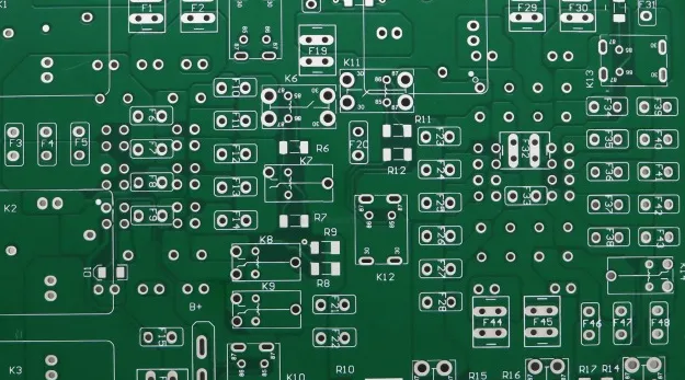
How HASL Is Applied
Once the fluxing is done, the fabricator exposes the board to molten solder. Air knives come into play here and remove the excess. The remaining layer protects copper and accepts solder willingly. Make a note that its height can be different across small pads.
How ENIG Is Applied
Now we’ll talk about ENIG. It deposits electroless nickel on copper. Subsequently, it finishes with immersion gold coatings. You don’t need any external current. Gold protects the nickel prior to assembly. Meanwhile, nickel provides the solderable barrier. [1]
How Their Coating Structures Affect PCB Performance
HASL leaves a thicker solder deposit. Drainage and air leveling affect it. ENIG is very close to the geometry of the pad. This is where most ENIG vs HASL flatness decisions come from.
ENIG vs HASL by PCB Design Requirement
BGA, QFN and Fine-Pitch Components
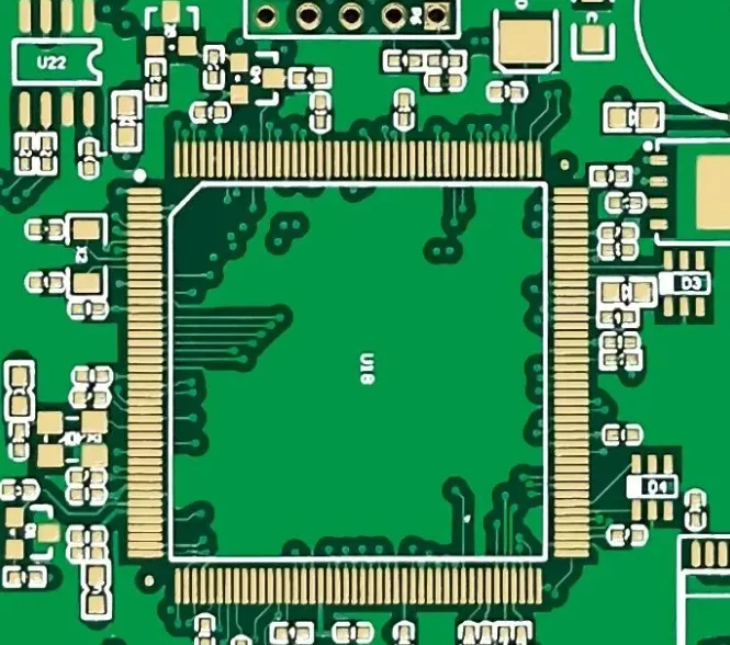
In the context of fine pitch packages, small differences in height are blown up. When it comes to BGA or QFN pads, a flatter finish helps in making consistent contact with the stencil, volume of the paste applied and coplanarity of the packages. ENIG might be preferred. But it's too coarse to say “BGA means ENIG. The possibility of using lead-free HASL depends on the pitch, the size of the circuit to be assembled, the mask's definition and the assembler's process window.
PCB Assembly and Solderability
Both fresh and controlled ENIG and HASL surfaces can be reliably wetted. As you know, HASL already places solder on the pad. What about ENIG? Printed pastes and miniature placement are based on a uniform base in ENIG. What seems to be more important than a general solderability ranking is the rework frequency consideration, stencil imprint and inspection characteristics.
Cost Sensitive PCB Production
Processing begins an ENIG vs HASL price comparison. ENIG needs numerous wet-chemical stages as well as nickel and gold control. So its fabrication charge might be higher. Gold averaged US$4,595.75/troy ounce during the first 7 months of 2026, adding material-price exposure to the ENIG production costs. But you should also remember that finish price isn’t total manufacturing cost. What if flatness reduces assembly defects or rework? ENIG may repay the premium. Regarding roomy SMT or through-hole boards, it can be needless over-specification.
Storage and Shelf-Life Requirements
ENIG’s gold saves nickel from oxidation. As a result, this is attractive when you find fabrication and assembly far apart. No need to attach a universal number of months to either finish. Packaging, contamination, moisture, ESD and solderability degradation are some of the associated concerns. And you know what? These concerns have been highlighted by the current IPC-1602 standard. You should inquire about how boards will be sealed, handled and stocked. [2]
Reference: IPC-1602A, Standard for Printed Board Handling and Storage
Reliability and Multiple Thermal Cycles
As indicated by Indium Corporation, a SAC305 reflow profile peaks between 240°C and 245°C. Therefore, reflow and rework cycles add thermal exposure that can be considerable. In the context of ENIG, it sidesteps molten-solder leveling during the fabrication process. However, it carries an ENIG-specific nickel-corrosion caveat which is called black pad. Consider that supplier process control issue. Joint life cannot be guaranteed by finish name alone. [3] [4]
Supporting sources: Indium Corporation SAC305 reflow application and PCB failure analysis related to the ENIG black pad problem .
ENIG vs Lead-Free HASL for RoHS-Compliant PCBs
If considered intentionally, there is no lead present in ENIG. Conventional tin-lead HASL does. But lead-free HASL makes use of a compliant alloy. This might be the relevant alternative for most RoHS projects. According to European Commission guidance, a 0.1% maximum lead concentration can be by weight in homogeneous material, subject to exemptions. Thus, the choice is lead-free HASL vs ENIG. And it is followed by cost, flatness and assembly checks. [5]
Regulatory source: Directive 2011/65/EU (RoHS), Annex II
ENIG vs HASL Thickness and IPC Requirements
IPC-4552B keeps an eye on ENIG for the context of soldering, wire bonding and contact finishes. Its rigid-board nickel range is 3 µm to 6 µm, or 118.1 µin to 236.2 µin, as per the Printed Circuit Engineering Association. The immersion gold controls per Rev A are in the range of 0.04 µm to 0.10 µm at specified statistical limits. HASL is less uniform by nature. So what you have to do is confirm coverage and acceptance criteria (not compare one nominal figure). [1]
Standard: IPC-4552B — Specification for Electroless Nickel/Immersion Gold (ENIG) Plating for Printed Boards
ENIG vs HASL Application Selection Table
| PCB Condition | Recommended Finish | Why | Key Condition |
|---|---|---|---|
| BGA, QFN or fine-pitch SMT | ENIG | Flat pad surface | Package type isn’t decisive |
| Simple SMT or through-hole | HASL or lead-free HASL | Adequate at lower cost | Check pitch of component |
| Cost sensitive prototype | HASL | Preserves budget | Dense packages may justify ENIG |
| Long storage before assembly | ENIG | Better oxidation barrier | Dry packaging is essential |
How These Standards and Studies Apply to PCB Selection
Application 1: Boards Stored Before Assembly
IPC-1602A shows why storage decisions should not depend on surface finish alone. Packaging, moisture exposure, storage environment, ESD control and handling conditions also affect the condition of the printed board before assembly.
Source: IPC-1602A
Application 2: ENIG Process Control and Black Pad Risk
ENIG can provide the flat surface needed for many dense SMT designs, but finish selection does not guarantee solder-joint reliability. IPC-4552B addresses ENIG plating requirements and nickel corrosion, while published failure-analysis research links ENIG black pad problems to defects and corrosion in the nickel/immersion-gold system.
Sources: IPC-4552B | Circuit World black pad study
Application 3: RoHS-Compliant Surface Finish Selection
For RoHS projects, conventional tin-lead HASL and lead-free HASL should not be treated as the same finish option. Directive 2011/65/EU sets the maximum concentration value for lead at 0.1% by weight in homogeneous materials, subject to applicable exemptions.
Source: Directive 2011/65/EU
FAQs regarding ENIG vs HASL
Does Every BGA or QFN PCB Need ENIG?
No. ENIG is the condition of use only if pad flatness is critical. You should also be aware of that the package label is only one input. Apart from that, you have to review pitch, land geometry, solder-mask definition, stencil design and assembly capability before you specify the finish.
If the PCB Will Be Stored Before Assembly Which Finish Is Better?
Suppose the gap between fabrication and assembly takes a bit longer. In this situation, ENIG can be picked. Even so, factors such as sealed packaging, humidity, contamination control as well as handling are what determine whether or not solderability endures storage. [2]
What Do I Need to Know to Recommend ENIG or HASL for My PCB?
An engineer needs to know about package types, minimum pitch, pad dimensions, SMT and through-hole content, reflow profiles, RoHS status, expected shelf life and production volume. These are the variables that disclose if ENIG’s characteristics create any actual value or not.
What Should I Provide If I Am Not Sure Whether I Should Specify ENIG Or HASL?
You can send us at KnownPCB your Gerber files, BOM, assembly drawing, component-pitch details, required quantity, compliance notes and storage expectations. Have any reflow, rework or reliability requirements that might be unusual? Very good! You can add them as well. That project package provides a defensible surface-finish recommendation and a precise quote.
Technical References
- IPC. IPC-4552B — Specification for Electroless Nickel/Immersion Gold (ENIG) Plating for Printed Boards.
https://www.ipc.org/TOC/IPC-4552B-toc.pdf - IPC. IPC-1602A — Standard for Printed Board Handling and Storage.
https://www.ipc.org/TOC/IPC-1602A-TOC.pdf - Indium Corporation. SAC305 reflow application using a peak temperature around 245°C.
https://www.indium.com/blog/reinforced-solder-preforms-for-high-reliability-and-low-voiding-voiding-doe/ - Ramanauskas, R., Selskis, A., Juodkazyte, J., Jasulaitiene, V. PCB failure analysis related to the ENIG black pad problem. Circuit World, 2013, 39(3), 124–132. DOI: 10.1108/CW-05-2013-0013.
https://www.emerald.com/cw/article-abstract/39/3/124/18426/PCB-failure-analysis-related-to-the-ENIG-black-pad - European Parliament and Council. Directive 2011/65/EU on the restriction of the use of certain hazardous substances in electrical and electronic equipment (RoHS). Annex II.
https://eur-lex.europa.eu/legal-content/EN/TXT/?uri=CELEX%3A32011L0065 - Mousavi, M., Kosari, A., Mol, J. M. C., Gonzalez-Garcia, Y. Localised aqueous corrosion of electroless nickel immersion gold-coated copper. Corrosion Engineering, Science and Technology, 2022. DOI: 10.1080/1478422X.2022.2096322.
https://doi.org/10.1080/1478422X.2022.2096322
The surface finish appears to be the easiest thing to decide before the quote gets locked in assumptions. Please allow us at KnownPCB to review the actual files and assembly conditions. After that, we’ll specify only the coating performance your PCB is truly in need of.