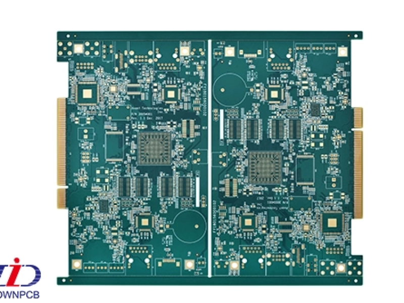
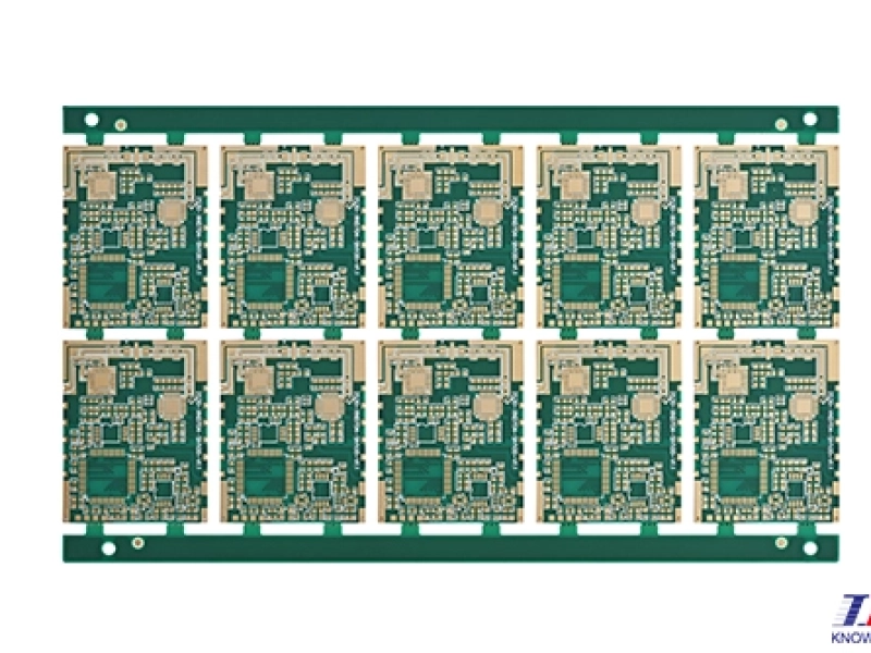
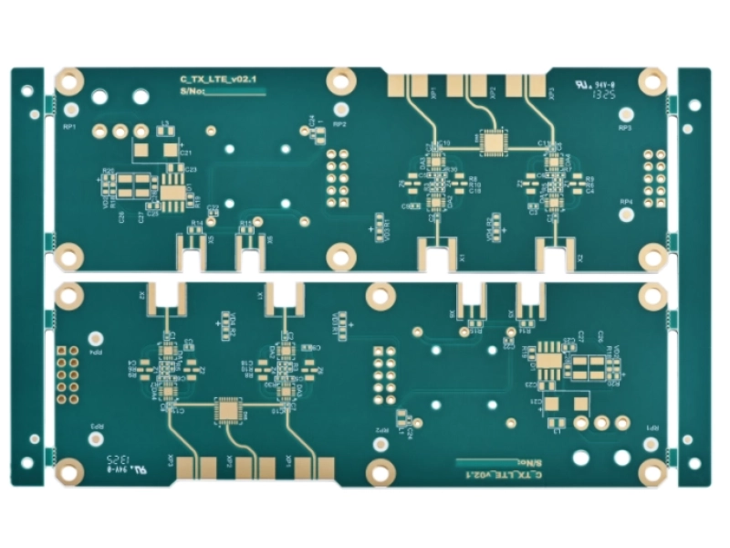
KnownPCB manufactured a 12-layer 5-step HDI PCB for a 5G smart terminal mainboard, this is a typical high density interconnect PCB case with complex blind/buried via structure, facing two main manufacturing challenges. Let's see how we solve the problems and how your HDI PCBs are made.
Project Background
Our client is a communication device supplier, they want us to produce 1000pcs 12-layer 5-step HDI PCBs for their 5G smart terminal mainboard.
Key Manufacturing Challenges of this 12-layer HDI PCB:
1. Layer registration and material movement control
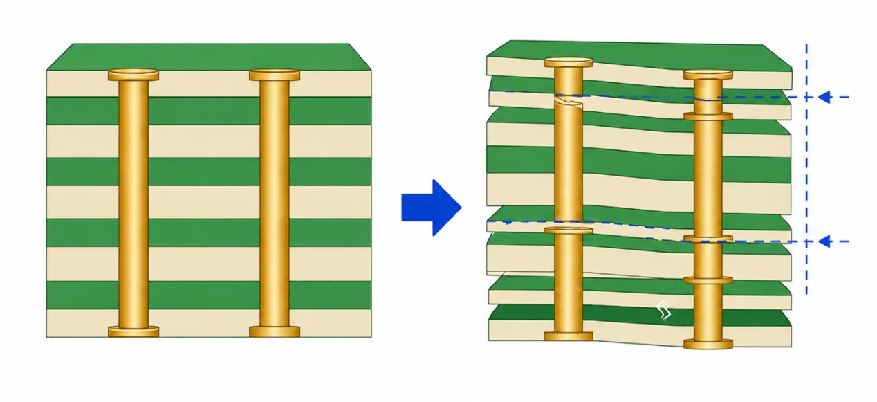
The 5-step HDI PCB structure means it requires 5 laser drilling and lamination cycles, each cycle causes material expansion and contraction, thus increasing the risk of layer misregistration, blind-via offset and material-related defects.
2. 35μm/35μm fine line and space
As we just said, the influences of 5 cycles are accumulated, high density PCB usually means pretty dense traces and fine space. In this project, the inner layer line and space is 35μm in the dense routing area, which makes it harder to keep accurate pattern during etch process.
HDI PCB Manufacturing Process
Once we confirmed the requirements with customers, KnownPCB engineering team would check all relevant files, including Gerber, drill, solder mask, stack-up, mechanical files, this is a critical DFM check before production. In this HDI PCB manufacturing case, our client provided necessary files and passed initial review, which meant the board is manufacturable.
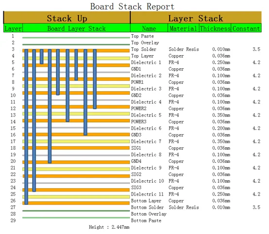
Then came the real factory process, the HDI PCB manufacturing process includes more than 30 steps strictly, we only talk about the typical processes of HDI PCBs here.
1. Inner Layer Imaging (LDI Exposure)
2. Sequential Lamination
3. Laser Microvia Drilling
Stacked microvia formation and filling
4. Via Filling / Copper Plating
5. Outer Layer Imaging & Plating
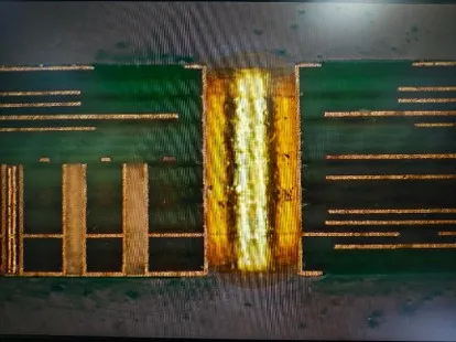
6. Microsection & Electrical Test
To verify via quality, registration and electrical integrity
7. Packing & Shipping
Watch the whole process of PCB manufacturing:
KnownPCB PCB manufacturing process
Final Thought
For this kind of complex HDI PCB projects, producing one PCB is not enough, keep the mass production consistently is more important and more challenging. At KnownPCB, the yield of this kind of HDI PCB is usually up to 95%. If you are evaluating a multilayer and multistep HDI PCB, send us your Gerber and stack-up for a DFM review.
Frequently Asked Questions
1. What is the difference between HDI PCB and normal PCB?
HDI PCB offers higher routing density and smaller vias, it uses space more efficiently compared with normal board.
2. How does HDI multilayer PCB improve signal integrity?
With HDI PCB's shorter interconnection, smaller microvias and better layer stackups, the parasitic inductance, signal loss and crosstalk of your design reduced.
3. When should you choose HDI PCB?
When your design contains fine-pitch BGAs, high I/O density, limited board space or high-speed signals, you should consider HDI PCB.
4. How to choose an HDI PCB manufacturer?
Experience is critical. Make sure they have proven capabilities in laser drilling, microvia formation, sequential lamination, via filling, layer registration and controlled impedance.