In high-density interconnect (HDI) stackup design, controlled impedance in HDI boards does not just start with trace width, it is also begin with the stackup. In real-world engineering and HDI manufacturing, KnownPCB summarized 4 critical linked factors that determine controlled impedance of a manufacturable HDI PCB:
1. Early HDI stackup definition
2. Trace grometry and dielectric spaing in a HDI circuit board
3. HDI manufacturing tolerance
4. HDI PCB Design-fabrication alignment and DFM review
These points together decide whether the impedance target can be defined clearly in HDI board design and stably achieved in HDI PCB mass production.
Impedance and stackup feature a interactive cause-and-effect relationship in the HDI PCB design.
1. From the perspective of HDI circuit board design planning, impedance dictates the stackup selection:
Core chips (CPU, DDR, 5G chips, etc) have specified clear impedance standards for signal transmission such as 50Ω and 90Ω from the beginning of the HDI board design stage, this is the foundation of the HDI stackup design, engineers should choose qualified the core materials for HDI PCB and optimized dielectric layer thickness.
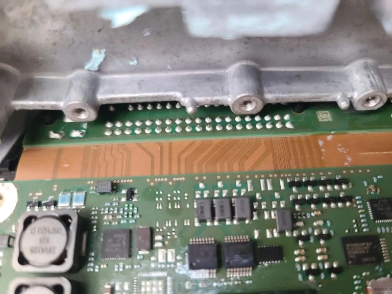
2. From the perspective of reality HDI PCB manufacturing, the stackup structure determines the performance of impedance: Impedance is a characteristic that presented during signal transmission in physical space.In practical fabrication, trace width (W) will generally adjusted in the later stage of stackup design, while the dielectric thickness (H) that is defined by stackup construction is the key physical basis for determing the fundamental impedance range.
Besides the trace width of a HDI board, the final impedance performance is highly rely on the dielectric spacing in the HDI structure. These geometric parameters are directly defined by the stackup design of HDI PCB.
The physical spatial relationship between signal layers and their reference environment, such as adjacent ground or power planes, will decide the stability of signal return path, which is significantly critical in high-density HDI routing.
Reference: For more information on reference continuity, please refer to Return-Path Stability as Part of HDI Stackup Design.
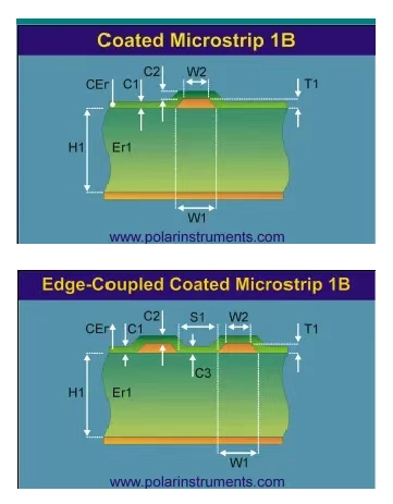
Typical impedance structures in HDI PCB design, showing how trace width (W), dielectric thickness (H), and spacing (S) together define the impedance environment.
Image reference from Polar instruments
The nominal impedance in the HDI PCB design phase is a theoretical terget. The final impedance of finishied HDI boards depends on manufacturing tolerance variations of stackup structural parameters. General impedance control capability is about ±10% and high-demand projects can achieve ±5%
As the professional PCB manufacturer, KnownPCB focus on controlling impacts of the following stackup variables:
1. Lamination Thickness Tolerance:
HDI boards require multiple times lamination. During the laminating process, resin flow of prepreg (PP) will cause deviation between the actual pressed dielectric thickness and the theoretical value under high temperature and high pressure, this is a key challenge for HDI stackup thichness management.
2. Copper Thickness Variation:
Blind via electroplating and outer layer copper plating will change the thickness on the top of traces. Such copper thickness changes can directly reshape the
structural correlation between signal traces and reference layers and also influence the impedance that defined by the HDI stackup.
3. Etch Compensation Tolerance:
In the etching process, lateral side etching will affect the trace.
We use process compensation to ensure the finished trace width is highly consistent with the impedance trace width that preset in HDI stackup design.
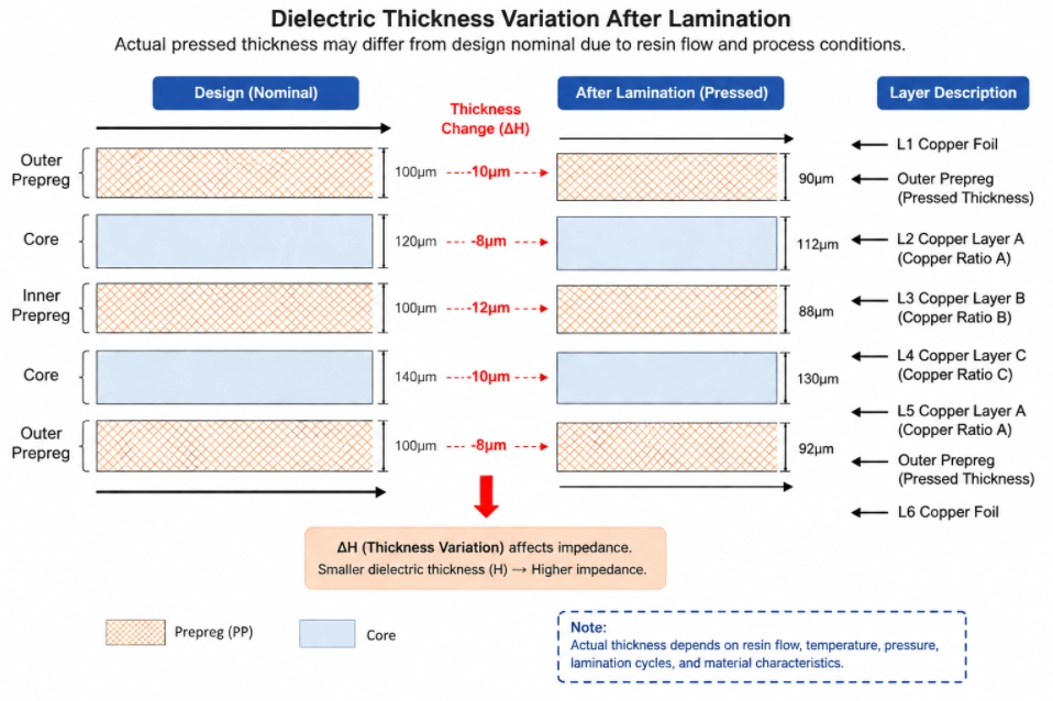
Variations in pressed dielectric thickness (ΔH) are one of the primary sources of impedance deviation.
Final impedance control depends on the cooperation betwwen the specifications of HDI stackup design and the PCB manufacturer’s process stabiliy.
As a key quality check step in the PCB manufacturing process, DFM review will align HDI board design layout with process capabilities of the practical production (such as the specific material resin flow and etching compensation factors).
Through the DFM review for the HDI stackup before circuit board manufacturing, we can proactively avoid risks of impedance deviation, and ensure the stability and reability of the target of HDI board design in the real HDI PCB fabrication environments.
Reference: To learn more influencing factors of HDI structures on the manufacturable HDI PCB, please refer to Common Stackup Choices For A Manufacturable HDI Board
Conclusion
Impedance control for HDI boards is not just about the calculation of trace width, it is a systematic engineering that base on HDI stackup design and manufacturing capabilities.
A HDI circuit board may be routed smoothly in design software, but the impedance stability can be effectively ensured when the HDI construction design closely matches with HDI board manufacturing process tolerances.
Request for a tech support
March/17/2026Industrial Impedance Control PCB Manufacturing
March/04/2026RFPCB Optimization for Ultrasound Probe Medical Devices
March/20/2026Automotive Multi Camera System Demands and Challenges in PCB Process

March/17/2026SMT Reference Board with Specialized PCB Fabrication
March/17/2026What is a metal core pcb in industry?
