KnownPCB provides end-to-end PCB assembly services covering SMT assembly, through-hole assembly, prototype PCBA, low-volume production, component sourcing, turnkey assembly, testing and online quote support.
Service Navigation
This page helps you quickly select the PCBA service that matches your project stage, assembly process, sourcing model and quote requirement. Click each service module to view detailed capabilities, workflow and technical information.
Suitable for early-stage engineering samples, design verification, functional testing and small-quantity PCBA trial builds.
Designed for NPI builds, pilot production, small-batch commercial orders and low-risk production before mass manufacturing.
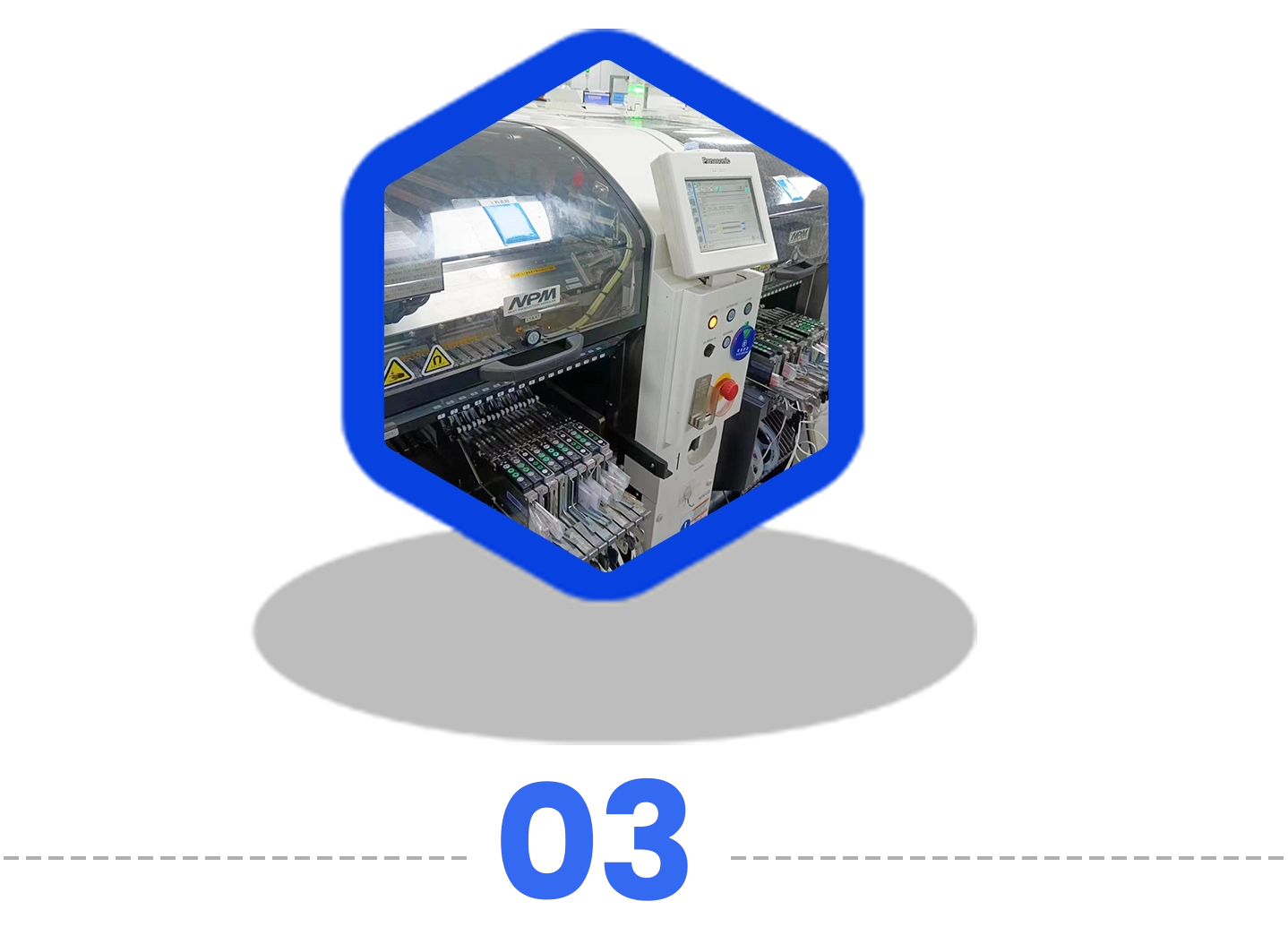
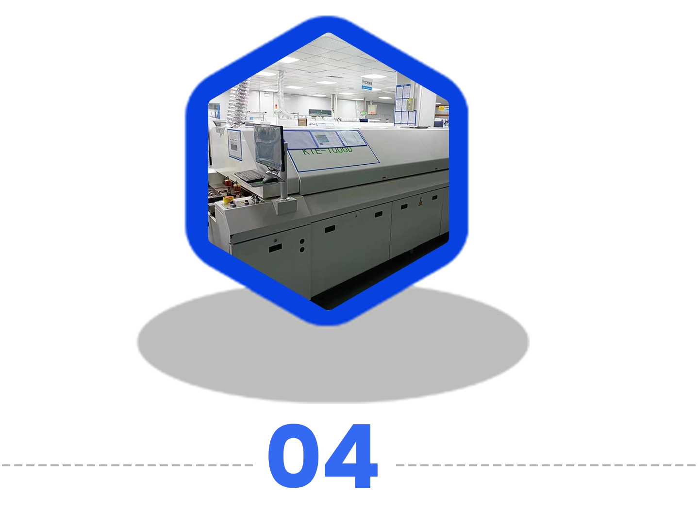
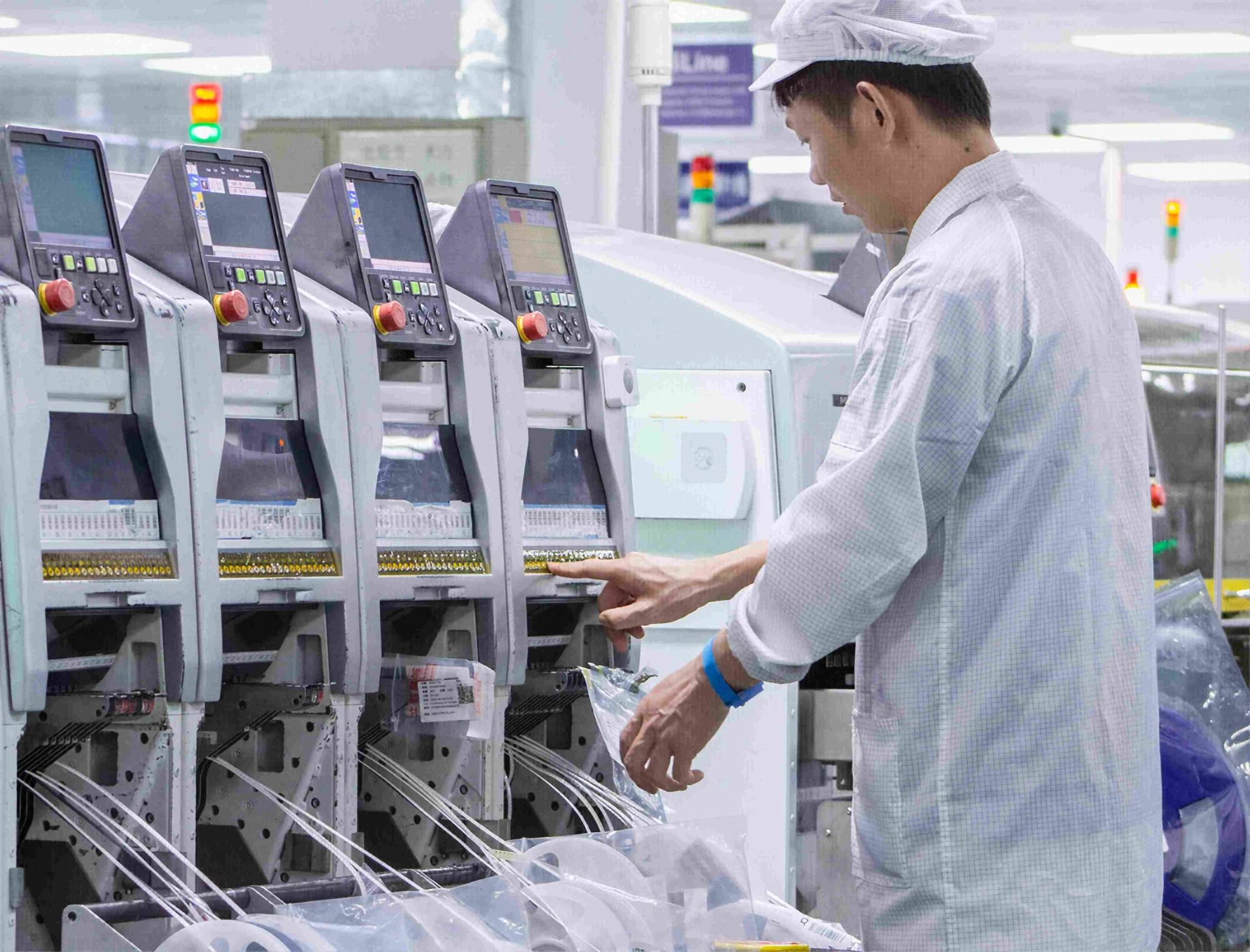
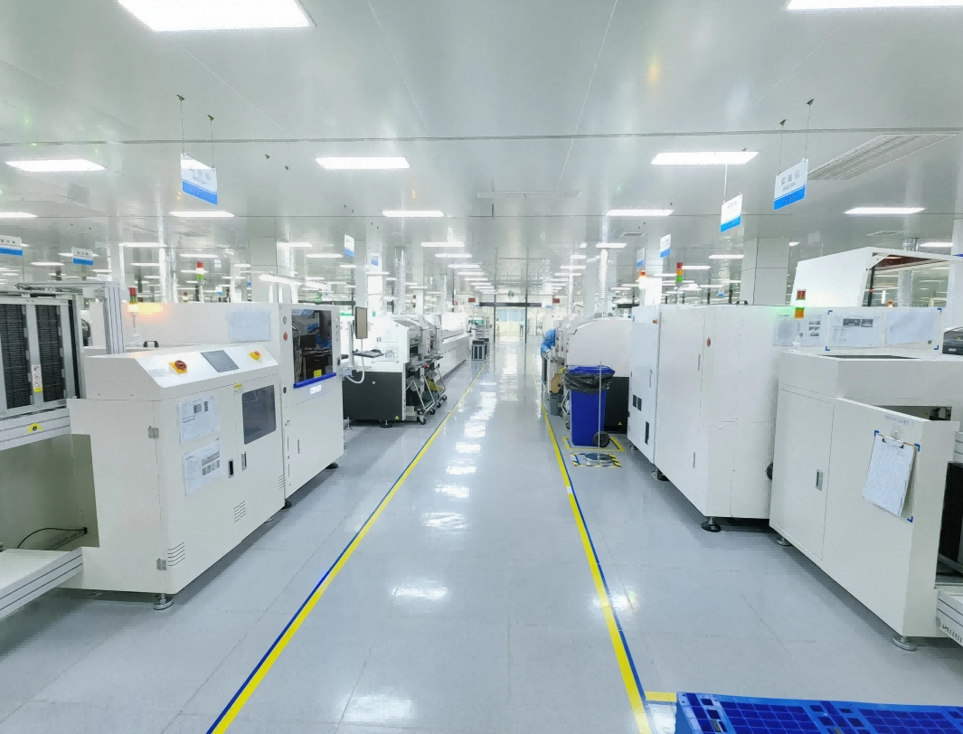
Covers solder paste printing, automated pick-and-place, reflow soldering, AOI inspection and X-Ray inspection for complex SMD packages.
Suitable for leaded components, connectors, transformers, switches, high-current parts and mixed SMT + THT assembly projects.
Helps customers manage BOM procurement, component alternates, shortage risks, lifecycle checks, incoming inspection and material preparation.
One-stop PCBA service covering PCB fabrication, component sourcing, SMT assembly, THT assembly, inspection, testing, packaging and delivery.
Use the online quote page when your Gerber files, BOM, quantity, sourcing model and assembly requirements are ready for cost and lead-time review.
Selection Guide
Use the table below to quickly match your project requirement with the correct service page. This improves user experience and helps customers enter the most relevant service page instead of reading unrelated content.
| Customer Requirement | Recommended Page | Best-Fit Scenario |
|---|---|---|
| First engineering sample, design verification or small test build | Prototype PCB Assembly | R&D samples, proof-of-concept boards, functional test boards |
| NPI production, pilot run or small-batch commercial order | Low Volume PCB Assembly | Low-risk production before scale-up, 10–1,000 pcs style projects |
| Surface-mount components, fine-pitch packages, BGA or QFN assembly | SMT Assembly Services | High-density boards, compact electronics, automated SMD placement |
| Leaded components, connectors, high-current parts or power devices | Through-Hole PCB Assembly | Industrial control, power electronics, mechanically stressed boards |
| BOM purchasing, component shortages, alternative parts or material control | Component Sourcing | Turnkey sourcing, partial turnkey sourcing, consigned inventory support |
| Complete PCBA delivery from PCB fabrication to testing and shipment | Turnkey PCB Assembly | Customers who want one supplier to manage fabrication, sourcing and assembly |
| Gerber and BOM are ready and the customer wants pricing or lead time | PCB Assembly Online Quote | Fast quotation, DFM check, file review and project evaluation |
Core Capabilities
KnownPCB supports prototype, NPI, low-volume and turnkey PCBA projects with engineering review, component sourcing, automated assembly, inspection and testing.
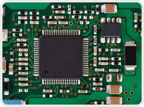
Review Gerber files, BOM, component footprints, spacing, clearances and manufacturability risks before production.
View prototype supportAutomated solder paste printing, pick-and-place, reflow soldering and inspection for fine-pitch and high-density boards.
View SMT detailsManual insertion, wave soldering and selective soldering for connectors, power devices and mixed-technology boards.
View THT detailsBOM validation, part alternatives, supplier coordination, material inspection and shortage-risk support.
View sourcing detailsFlexible PCBA production for pilot runs, small-batch orders, market testing and NPI production.
View low-volume assemblyComplete support from PCB manufacturing and material procurement to assembly, inspection, testing and delivery.
View turnkey assemblySPI, AOI, X-Ray, electrical testing and functional checks help verify solder quality and board performance.
Send testing requirementsSubmit Gerber, BOM, quantity, sourcing model and technical notes for quote and lead-time review.
Get quote nowTechnical Specifications
The following table summarizes standard and limited assembly capabilities for SMT, DIP wave soldering and conformal coating processes.
| Item | Sub-item | Standard Capability | Limited Capability | Remark |
|---|---|---|---|---|
| SMT Process | PCB - Min Size | L≥30mm, W≥30mm | L<30mm, W<30mm | BOT, TOP side components; Fiducial Mark should be ≥3mm from the board edge |
| PCB - Max Size | L≤650mm, W≤400mm | L:800-650mm, W:400-450mm | ||
| PCB - Component Thickness | 0.5mm ≤ T ≤ 3mm | T < 0.5mm, T > 3mm | ||
| Component Size - Min Package | 0201 (0.6mm × 0.3mm) | 01005 (0.3mm × 0.2mm) | ||
| QFP, QFN, SOP, SOJ - Min Pin Distance | 0.4mm | 0.3mm ≤ Pitch < 0.4mm | ||
| CSP, BGA - Min Pitch Distance | 0.4mm | 0.3mm ≤ Pitch < 0.4mm | ||
| DIP Process (Wave Soldering) | PCB Size - Min Size | L≥30mm, W≥30mm | L<30mm | |
| PCB Size - Max Size | L≤650mm, W≤400mm | L:800-650mm, W:400-450mm | ||
| PCB Size - Thinnest Size | 0.4mm | T < 0.4mm | ||
| PCB Size - Thickest Size | 5mm | T > 5mm | ||
| Conformal Coating Process | Temperature Range | -30℃ ≤ T ≤ 120℃ | -50℃ ≤ T ≤ 150℃ | |
| Coating Thickness | 20um ≤ T ≤ 35um | 35um ≤ T ≤ 60um |
Process Overview
This process overview helps customers understand how KnownPCB manages PCBA builds. Detailed SMT, THT, sourcing and turnkey workflows are available on the linked service pages.
Process: Validate Gerber, BOM, footprint accuracy and manufacturability before assembly.
Requirements: Correct footprints, spacing, clearances, thermal relief and DFM/DFA compliance.
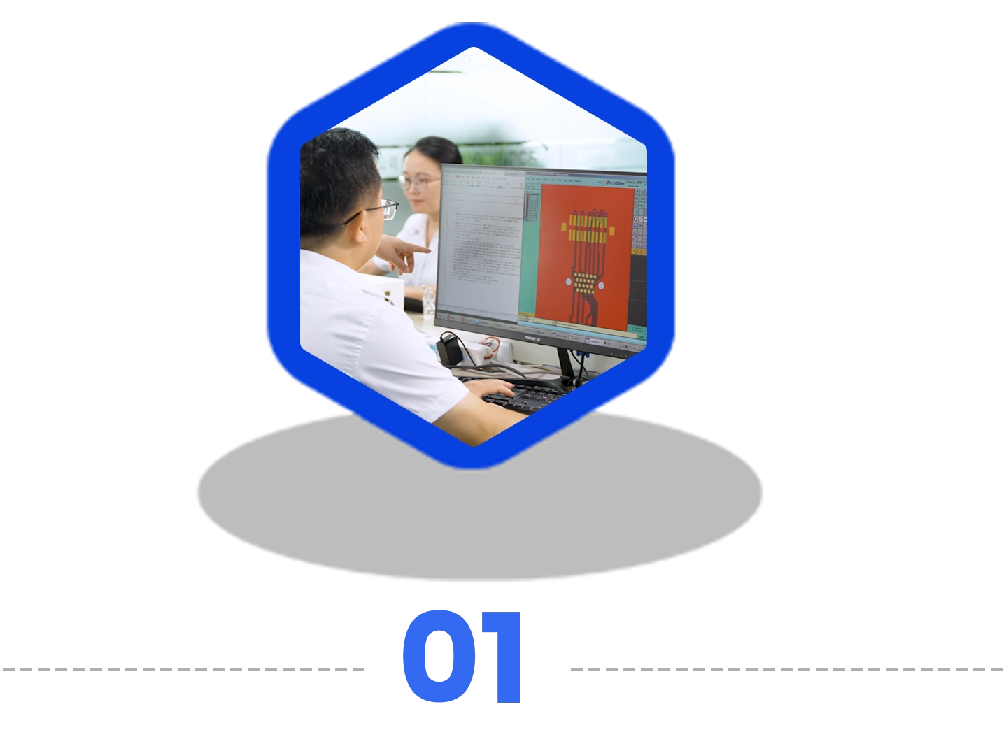
Process: Apply solder paste to SMT pads using stencil alignment and controlled deposition.
Requirements: Laser-cut stencil, paste viscosity control, 2D/3D SPI and uniform paste volume.
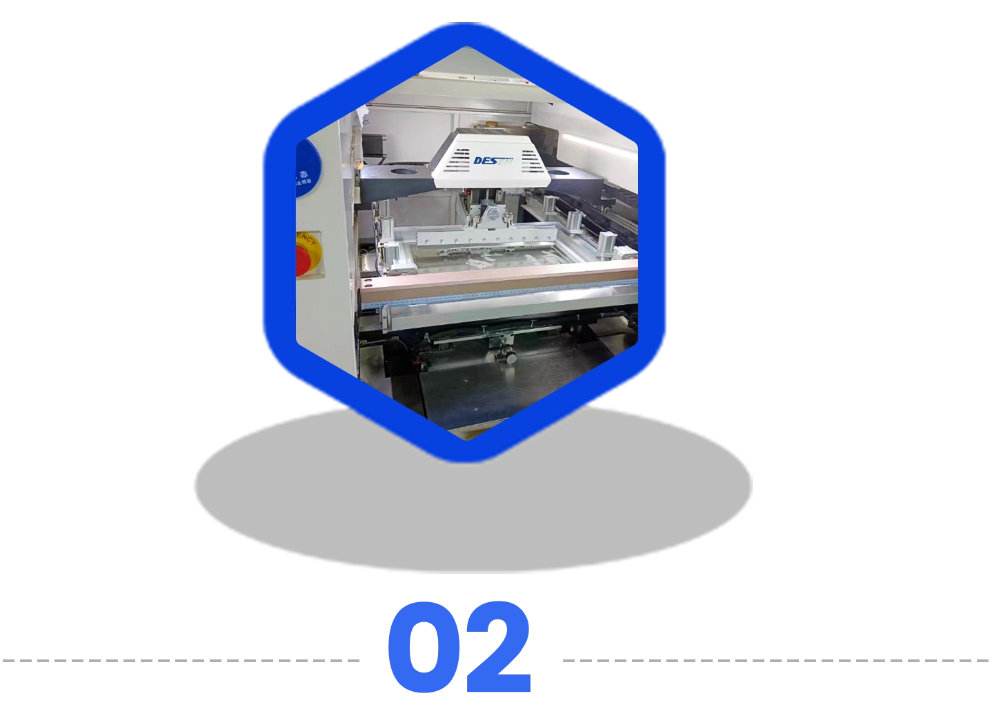
Process: Place SMD components with automated pick-and-place and vision alignment.
Requirements: Feeder calibration, optical centering and fine-pitch handling for BGA/QFN/01005.
Process: Melt solder paste under controlled thermal profiles to form reliable solder joints.
Requirements: Multi-zone profiling, peak temperature control, soak control and cooling control.
Process: Insert leaded components manually or automatically, then solder by wave or selective process.
Requirements: Lead forming, wave height control, hole-fill quality and solder fillet inspection.
Process: Remove flux residues and apply optional conformal coating when needed.
Requirements: Ionic contamination limits, coating thickness control and masking of critical zones.
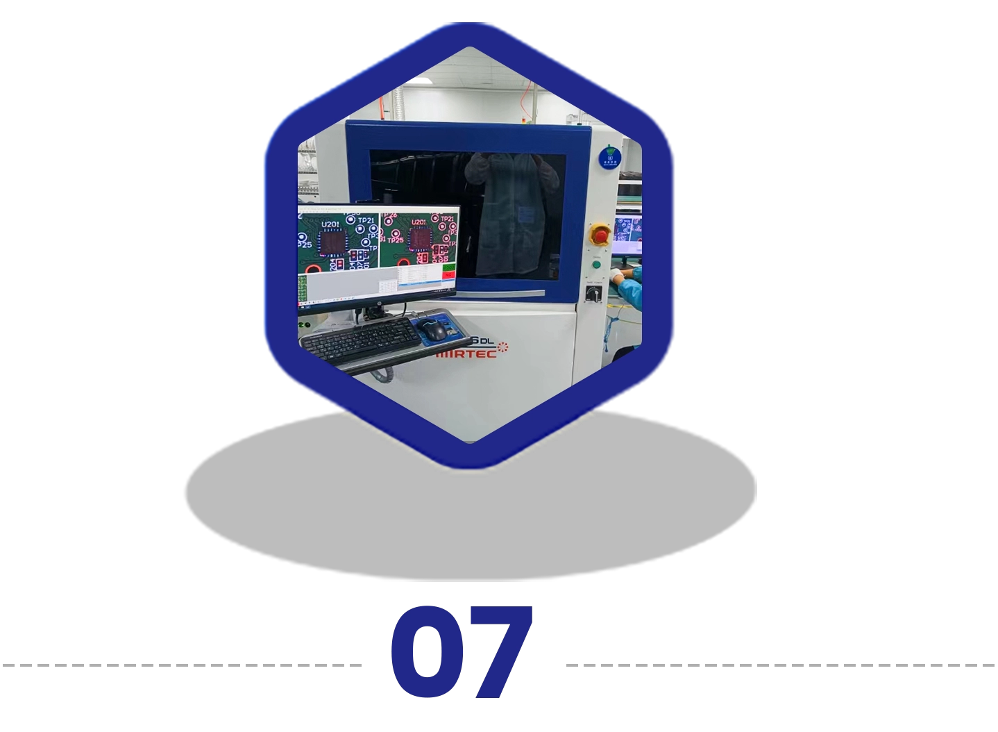
Process: Verify assembly quality using AOI, X-Ray, ICT, flying probe or functional tests.
Requirements: AOI coverage, X-Ray for BGA, test-point design and electrical validation.
Send your Gerber, BOM, drawings and assembly notes to let our engineering team review the best process route.
Start a QuoteKnownPCB supports complete material procurement through component distributors, BOM validation, lifecycle checks, alternative part review, incoming inspection and traceability control.
Quality control is applied across file review, material preparation, SMT assembly, THT assembly, inspection, testing and final shipment.
Applications
KnownPCB supports PCBA projects for industrial, IoT, medical, automotive, telecom, aerospace and power electronics applications.
Assembly support for automation controllers, control boards, sensor modules and industrial electronics.
Prototype and low-volume PCBA for connected devices, smart hardware and compact electronic products.
Assembly support for medical electronics requiring stable quality, traceability and controlled process review.
PCBA support for power, control, charging, monitoring and automotive electronic modules.
Assembly for high-speed communication, networking, RF-related and connectivity products.
Engineering-focused PCBA support for reliable and complex electronic assemblies.
FAQ
Choose prototype PCB assembly if you are building first samples or engineering validation boards. Choose low-volume PCB assembly if your design is more stable and you need pilot production, NPI builds or small-batch commercial production.
SMT assembly is suitable when your PCB uses surface-mount components such as resistors, capacitors, ICs, QFN, BGA, LGA, CSP or other fine-pitch SMD packages.
Through-hole assembly is commonly used for connectors, switches, transformers, high-current components, power devices and parts that need stronger mechanical bonding than standard SMT components.
Yes. KnownPCB supports component sourcing, BOM validation, shortage review, alternative part suggestions and material preparation for turnkey, partial turnkey and consigned PCBA projects.
To request a quote, customers usually provide Gerber files, BOM, pick-and-place file, assembly drawing, quantity, sourcing model, testing requirements and any special process notes.
Upload your Gerber files, BOM and assembly requirements. KnownPCB will review your files, check manufacturability, evaluate component sourcing options and provide PCBA pricing and lead-time support.
