8 Layer PCB Stackup Design Problems and Solutions
Summary: This article discusses when to use 8 layer PCB stackup, common troublesome design problems, two design cases, via cost comparison, layer calculation guidance, thickness, references, and author information.
1. Intro
Considering that 8 layer PCB stackup is previously in high demand, we will look into some troublesome design problems in this article. Also, discussions about layer calculation are included.
2. When Should I Use 8 Layer PCB Stackup?
Depend on what the end product is.
- High-speed digital circuits: For PCIe Gen4/5, DDR4/DDR5 memory, and SerDes (serializers/deserializers).
- High-performance computing equipment: server motherboards, workstations, AI acceleration cards.
- Communication infrastructure: 5G base stations, optical modules, network switches.
- Automotive electronic systems: Specifically, ADAS (Advanced Driver Assistance Systems), in-vehicle Ethernet, radar.
- Industrial Automation and Medical Equipment: PLCs, industrial robots, and imaging devices like CT/MRI.
3. What Is the Main Problems of 8 Layer PCB Board Stackup?
According to our record, 6 types of problems can be classified as followed.
3.1 Fabrication Capability (42.4%)
Line width, line spacing, hole diameter, copper ring, HDI, blind buried hole, back drilling, Via-in-Pad, thick copper
3.2 Signal Integrity (18.2%)
Impedance control, high-speed signals, laminated structure, EMC, via stub
3.3 Thermal & Power (15.2%)
Heat dissipation through-hole, thick copper, high current, copper column, high thermal conductivity structure
3.4 Material & Reliability (12.1%)
High Tg, mixed pressure, thermal cycling, material change
3.5 Assembly/SMT (9.1%)
Solder bridges, BGA, surface treatment
3.6 Compliance & QA (6.1%)
IPC Class 3, medical and military industries, 100% AOI/electrical testing
4. Case 1: I Feel a Bit Fragmented for the Power Distribution of My 8 Layer PCB Stackup Design.
Take a case from the above type 2 signal integrity.
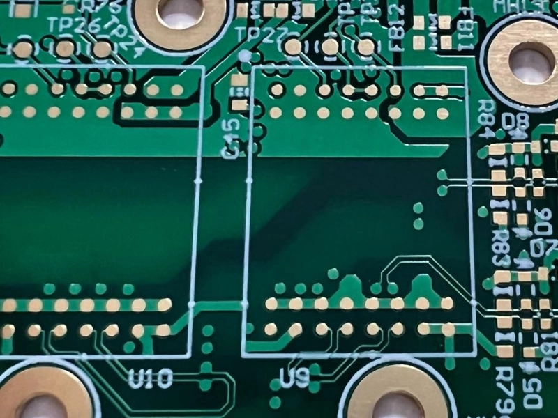
One of our clients sent us his 8 layer PCB design draft. It looks very pretty for the stack up, including signal, GND, signal, power, power, signal , GND and signal, total 8 layers. It is a very classical design, but he feels the power distribution is a bit fragmented. Also, the return paths are in some dense areas.
One outstanding point caught our attention. Now the ground layer design is like
Put the return current continuity first. For high-speed PCB design, signal actually rely on return current continuity, but not power plane. Only one GND via, which is not a perfect conductor, carries inductance and impedance.
As a saying goes, the return current of high-speed signals always prefers the path with lower impedance. KnownPCB engineers suggest more than one GND via. The return inductance would be shared by parallel via.
1/L_total = 1/L1 + 1/L2 + ... The signal, in this way, can clearly return through a less impedance path.
5. Case 2: Too Aggressive Routing Around the BGA for My 8 Layer PCB.
Another case is from both type 1 fabrication ability and type 2 signal integrity.
Some design drawings we received show too aggressive routing around the BGA.Why? They commonly attribute to better fanout, following a series of challenges.
- Less integrity of power plane. Split plane for more routing space.
- Unsatisfied return path quality due to split plane.
There should be a balance between routing space and reference plane integrity.
HDI solves these problems to some degrees. Especially in smart phones and 5G devices, high density interconnect technique plays a key role. Take one of the HDI approaches for example.
Traditional fanout needs a short trace from the center of the BGA pad and through-hole via, while HDI allows direct connection. The simplified structure saves space for fanout and split for plane.
6. How Is the Cost to Solve This Problem Frequently Occurred in 8 Layer Board Stackup Design?
Undoubtedly, through hole via is the cheapest technique, but it can not save space and fragment of the plane. As I have handled before, 5 types of vias technique is recommendable for 8 layer stackup. And their costs vary.
| Via Type | Comparable Cost | Helpful to Plane Integrity | Application | Manufacturing Process Complexity | Manufacturing Challenges |
|---|---|---|---|---|---|
| Blind Via | 1.2~1.6times | Good | Medium-High Density Board | Middle | Depth-Controlled Drilling |
| Buried Via | 1.3~1.8times | Good | High-Density Internal Interconnects | High | Multiple Pressing Cycles |
| Microvia (Laser) | 2~5times | Excellent | HDI / smartphone/ DDR | Very High | Laser Drilling |
| Via-in-Pad | 3~8times | Excellent | Fine-pitch BGA | Very High | Hole Filling |
| Any-layer HDI | 8~16times | Excellent | Mobile Phone Motherboards / AI Modules | Very High | buildup |
If feeling no idea on how to choose via type at an appropriate cost level, ask KnownPCB for professional customized solution.
7. Conclusion
To sum up, 8 layer PCB can be applied to lots of industries, especially high-speed fields. Although headache problems confuse us, there are specific solutions after all. From design to manufacturing, lots of things need to be balanced, like cost, routing space and PCB performance. With the development of technology, high-speed products have a bright future.
FAQ
1. How Can I Calculate My Layer PCB Stackup?
If you want brief guidance for a quick look, I would like to share an experience based on industries.
- 2-layer PCB is mainly for LED, battery, simple MCU and low-speed product.
- 4-layer PCB is for Ethernet and common industrial controllers.
- Middle speed product can be matched 6-layer PCB, like double data rate 3 synamic random-access memory.
- Standard 8 layer PCB stackup can be applied in advanced driver assistance systems, system on chip, static random access memory.
- PCB with more than 8 layers can be used in CPU, AI models, GPU.
2. How Can I Calculate PCB Stackup Layer Step by Step?
If you would like to calculate step by step, you can start from listing the complexity of the PCB component, such as BGA pitch. Then think about whether the routing channel is enough. Still take BGA 0.5mm for example, 2 trace or channel is not enough for fanout routing in this case. So the next step is to think about adding layer or HDI. Besides that, reference plane should be added near every signal layer. Power planes should be completely added if you have 1.0V rail.
Now we have a rough concept for the layer calculating. Some common stackup structure should be remembered in mind for reference.
Do not forget to check the return path and routing congestion in the last step.
3. How Much Is 8 Layer PCB Thickness?
Between 1.0mm and 2.0mm. Depend on the copper foil thickness, insulating layer thickness, drilling and gold plating. Any questions, feel free to contact us.
References
- High-Speed Digital Design: A Handbook of Black Magic
Johnson, H., & Graham, M. (1993). High-speed digital design: A handbook of Black Magic. Prentice Hall. - IPC
IPC. (2022). IPC-2221B: Generic standard on printed board design. IPC Association Connecting Electronics Industries. - Printed Circuits Handbook
Coombs, C. F., Jr., & Holden, H. T. (Eds.). (2016). Printed circuits handbook (7th ed.). McGraw-Hill Education.