Blog & Design Guide

“How much current can this trace carry” is a main part of the topic about high-current PCB. This can easily lead to the impression that high-current PCB design is mainly about designing traces to carry more current.
An electronics’ current has to move through a complete path:
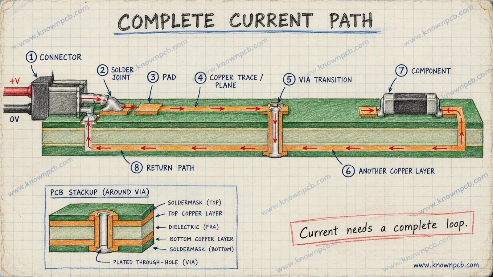
That bottle-neck section with a narrow trace needs extra copper—it's driving up resistance and causing heat dissipation.
But it is not the correct answer.
KnownPCB’s practice dedicated that design the current path first, and the rest of the PCB around it.
It’s basically what European high-current PCB manufacturer KSG does— they advocate defining high-current conductors before routing the logic portion of the PCB. Its published design sequence—you first move should be mechanical constraints, power-component placement, current requirements and ambient conditions, then build around defining layer structure and routing the remaining circuit.
Please clearly look at continuous and peak current first. But it is not just about the current, are you also factoring the thermal limits?
For example, just saying “100 A doesn’t tell us how much copper is needed, the spec alone won’t tell you the exact copper thickness. Let’s be honest, same 100 A design can look completely different, depending on your thermal limits and high-current PCB space, then plus how your stack-up and the connectors are set up.
A word of caution: Before you run an accurate initial high-current PCB assessment, we recommend defining these five inputs:
| High-current PCB design factors | What it determines |
|---|---|
| Continuous current | Required continuous current-carrying capacity |
| Peak current + duration | Whether short current peaks need separate consideration |
| Allowed temperature rise | How much conductor heating is acceptable |
| Available PCB area | Whether current can be handled with wider copper or needs another solution |
| Current entry/exit points | Whether connectors, pads, vias, or layer transitions may become bottlenecks |
In our experience, please don’t pick 2, 4, or 6 oz copper from the current rating alone. We lock in the current and thermal limit before choosing the conductor structure.
Remark: KSG's current carrying capacity method accounts for several factors, temperature conditions, PCB technology, pcb stack-up, and the number and how many high-current traces you actually have. Their high-current calculator asks for more than just current, you have to throw in ambient temperature, max PCB temp, max continuous current as well.
Actually, high-current PCB design is a coupled equations problem. There are a lot of interdependent factors—thermals, space, and stack-up all play together.
If you've ever dealt with a 30 A path on one high-current PCB, it can be harder to implement than a much higher-current path on another PCB board if:
That is why high-current PCB design should be treated as a cross-section and thermal-management problem.
Let’s break down the “COMPLETE path”, don’t forget the whole loop.
Recommended current-path model:
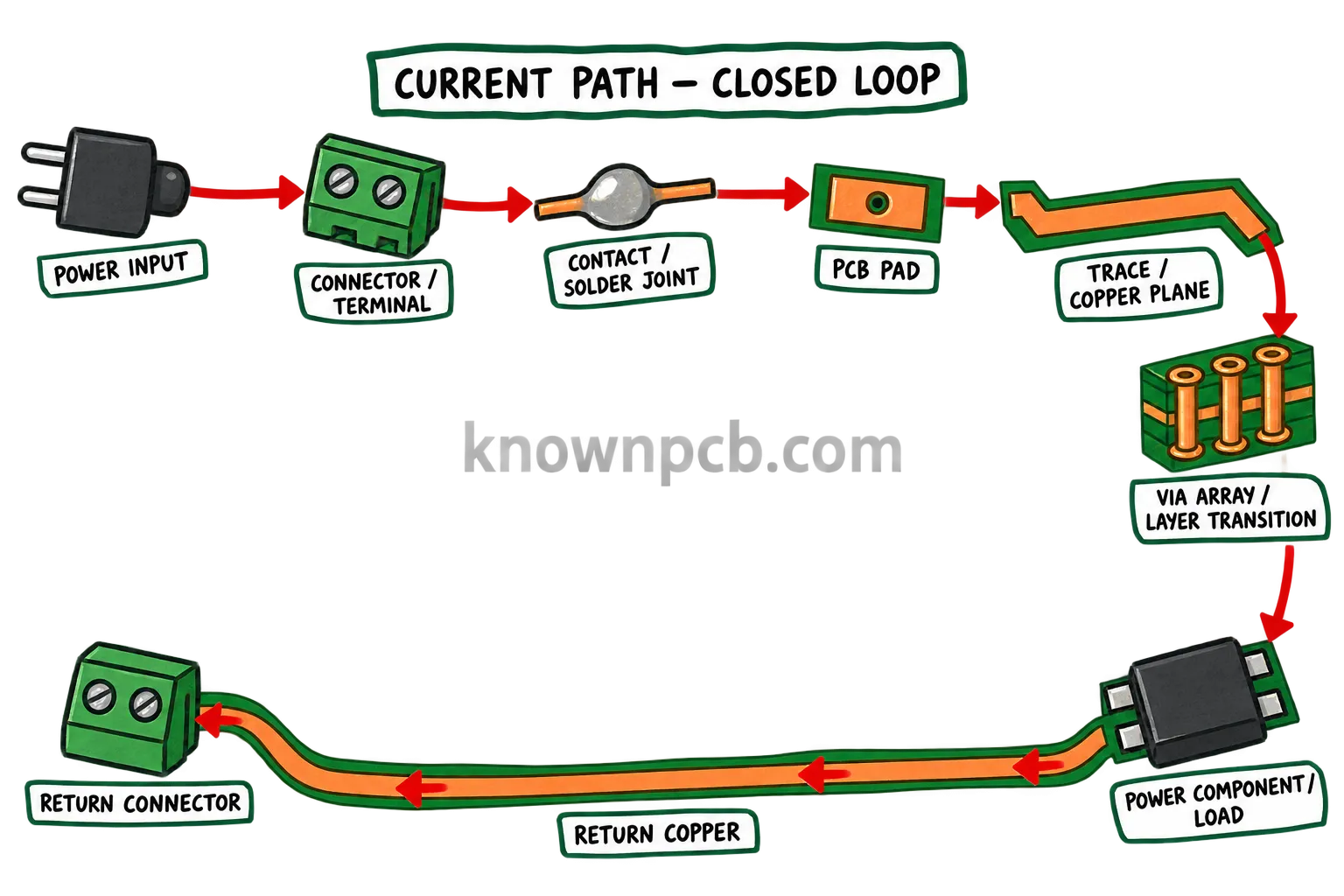
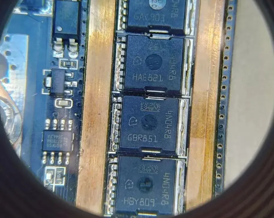
In practice, we should have a clear sense of “ the Bottleneck Effect”. the most impressive copper plane on the high-current PCB always means nothing if current is forced through, it won’t fly if you force 40 Amps through 4 tiny vias.
Remark: Cadence deal with high-current paths straightforward: They build up conductor volume across layers, multi-layer routing when you’re pinched for space on a single layer and simply can’t get enough copper width.
Look for the narrowest electrical cross-section.
This sounds obvious, but many high-current layouts visually look “heavy duty” while still containing one or two bottlenecks.
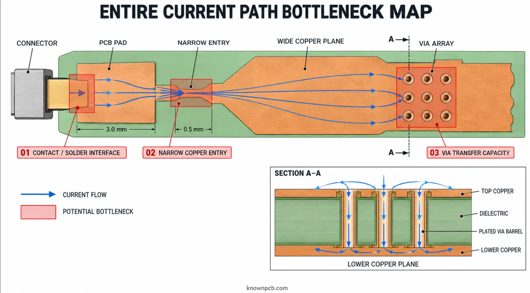
| Current-path location | What can go wrong |
|---|---|
| Connector contact | High contact resistance |
| Solder joint | Localized heating |
| Pad entry | Current crowding |
| Trace neck-down | Reduced copper cross-section |
| Via transition | Insufficient vertical copper |
| Plane split / corner | Uneven current distribution |
| Component terminal | Local thermal concentration |
| Return path | Unexpected resistance and current concentration |
If the bottleneck occurs at a layer transition, see our High-Current PCB Via Design Guide for via diameter, barrel copper thickness, via resistance, via count, current sharing and temperature-rise considerations.
Most PCB engineers stick to a simple rule of thumb: 10 to 15 mils of trace width per Amp on standard 1 oz copper. That’s why we use the formula: A wider trace simply gives amps more elbow room, dropping the resistance. But we cannot blindly widen the trace, components get squeezed right up against the trace.
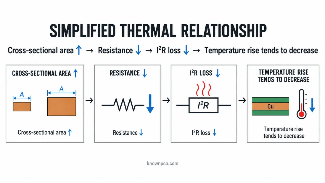
The design variable begins when it gets converted into rules such as:
Without conditions, we consider that statement incomplete.
Here is an example,
By IPC-2152, a 10 mm outer trace on 1 oz copper drops around 12 to 13 amps at a 10-degree rise.
But if we bump it up to 2 oz copper, we double the cross-section. So with a 20-degree rise, a 10 mm outer trace easily handles 22 to 25 amps, if not more.
The allowable current depends on variables including:
Remark: Altium's trace-width guidance similarly centers the calculation on keeping conductor temperature within an acceptable limit for a specified current.
We recommend to check actual PCB manufacturability (Confirm with your high-current PCB manufacturer)
If the high-current PCB board space permits, we generally prefer using more conductor width before automatically moving to very heavy copper.
Why?
Because thicker copper solves one problem but introduces manufacturing trade-offs.
To fit tight spatial limits, we offset reduced trace widths by increasing copper weight, preserving the net cross-sectional are.
However, heavy copper also affects fabrication geometry.
KSG notes that thick copper structures experience stronger undercut during etching, which limits how fine the conductor structures can be. Its published thick-copper capability uses 105–400 μm copper structures and explicitly ties achievable conductor geometry to final copper thickness.
If the board has enough physical area:
use geometry intelligently before using copper thickness as a brute-force solution.
If the high-current PCB board does not have enough area:
then heavy copper, parallel copper layers, embedded copper structures or a busbar-type solution becomes worth evaluating.
Evaluate localized copper reinforcement / busbar / hybrid structure
Notice that there is no universal ampere threshold in this flow.
That is intentional.
If increasing copper thickness becomes part of the design solution, compare the required conductor geometry with KnownPCB Heavy Copper PCB manufacturing capabilities before finalizing trace width and spacing.
| Finished copper | Typical production range | Min trace/space under your process |
|---|---|---|
| 2 oz | BASIC (2–3 oz) | ≥0.15 mm |
| 3 oz | BASIC (2–3 oz) | ≥0.15 mm |
| 4 oz | ADVANCED (4–6 oz) | ≥0.25 mm |
| 6 oz | ADVANCED (4–6 oz) | ≥0.25 mm |
Using multiple copper layers in parallel can be an effective solution, especially when one layer cannot provide enough conductor area.
Cadence explicitly recommends connecting high-current conductors across multiple layers with via arrays where one layer cannot accommodate sufficiently wide power traces.
But our position is: parallel layers only help if the current can actually enter and leave those layers efficiently.
A 4-layer high-current PCB doesn’t magically create four equal current paths.
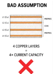
The current piles onto the widest, closest highway. That’s “Current takes the path of least resistance.” Think about pouring 4 copper layers, the 4 layers split your 50 Amps, but the connectors is soldered to the top layer. Well, current takes the lazy route, and won't naturally balance itself out, leaving your inner layers and vias totally underutilized.
To head off this nightmare upfront, if your multilayer high-current solution depends on several layers working in parallel, we proactively switch to a Thru-Hole connector to solve the Layer-to-Layer issue, or by staggering the via layout or dropping teardrops at the transition zone to smooth out current crowding.
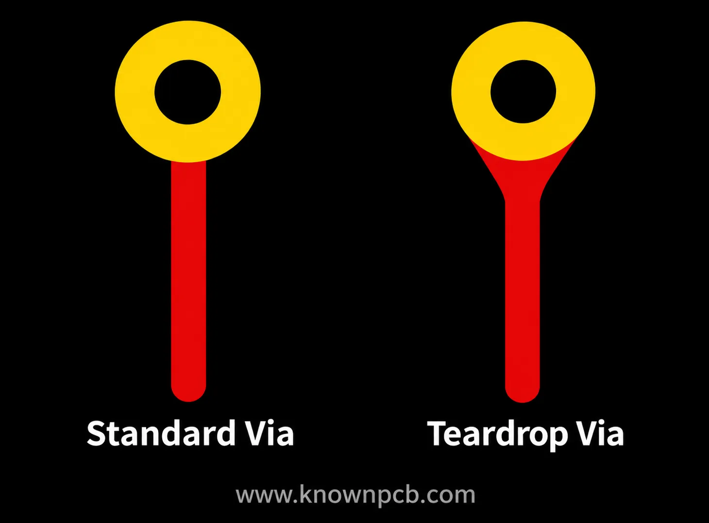
It is not wrong. “Add more vias” is one of the most common pieces of high-current PCB advice.
Altium notes that while PCB trace current capacity has received substantial standardization and study (Refer to IPC-2221), but when it comes to vias, the standards leave you in the dark. Because via current capacity has historically been less directly covered, it is a multi-variable trade-off matrix. Via thermal and current behavior deserves separate analysis.
Here are 3 multi-variable factors that should be considered.
3.1 add teardrops
3.2 By Deploy Via Arrays / Stitching Vias
3.3 Via-in-Pad with Larger Drill & Thicker Plating (bump up the via drill size or request heavy barrel plating)
To wrap it up, when you're sizing vias for heavy current, here are the core knobs as your preliminary reference:
For detailed calculations and design trade-offs involving via diameter, barrel copper thickness, via resistance, number of vias, current sharing and temperature rise, continue with our High-Current PCB Via Design: Current Capacity, Via Size & Via Arrays.
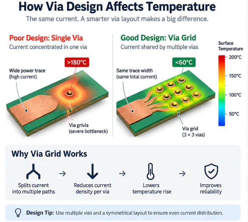
How Via Design Affects Temperature
Once the via geometry is defined, the next question is whether drilling and plating can reproduce the required barrel copper and hole geometry consistently. Continue with our High-Current PCB Via Manufacturing, DFM, Plating & Reliability Guide.
High-Current PCB Via Design: Current Capacity, Via Size & Via Arrays
High-Current PCB Via Manufacturing: DFM, Plating & Reliability
If your design includes heavy copper, multiple power layers, via arrays, MOSFET power paths, or strict temperature-rise limits, review the complete current path together with stackup and manufacturing constraints before production.
Request an Engineering Review Explore Industry SolutionsIPC-2152 — Standard for Determining Current Carrying Capacity in Printed Board Design
KSG — Current Carrying Capacity: Calculation & High Current Management
Cadence — Optimizing for PCB Trace Thickness vs Current Capacity
By Amy Jiang,
18-year sale engineering experience in PCB industry. A versatile sales engineer with both engineering background and international project experience. She is familiar with HDI, high-speed boards and small-to-medium batch manufacturing requirements. Being capable of quickly understanding the design pain points of customers and providing a one-stop PCB solution from DFM to mass production.
October/21/2026RO4350B vs RO4003C: Dk, Loss and Material Release
October/10/2026Power Supply PCB Creepage and Clearance: DFM Review

May/21/20268 Layer PCB Stackup:Headache Design Problems and Cost
October/15/2026Stacked vs. Staggered Microvias: Choose by Constraint
April/29/2026Key Perspectives for Industrial-grade PCB
Proven by 7 industries, 4000+ customer projects
Please contact us at sales@knownpcb.com, ask for engineering support here or use the form below to reach out to KnownPCB | Request a Manufacturing QuoteInclude your quantity, target delivery date and key requirements. File handling and NDA information. |