Blog & Design Guide

Power supply PCB component placement starts with the board outline and isolation boundary. The positions of the transformer, MOSFET, rectifier and capacitors also set the routing exits and thermal space available on the board. Fix the enclosure and connector constraints first, then place the transformer and power parts, and finish by checking small-signal routes, mounting points and fabrication data. This article uses transformer-based isolated supplies as context. It does not replace safety-distance calculations, magnetic design or component selection.
KnownPCB's power supply PCB page covers related board types. It is not a circuit example or a verified converter design for this article.
Table of contents
Power-board connectors often follow enclosure openings, cable direction and fixed mounting points. Set the outline, input and output connectors, screw holes, standoffs and heatsink contact surface first. Then place the transformer and large power packages. This prevents a layout from blocking screw access or leaving a connector plug in conflict with a capacitor or heatsink.
Check component height as well. A transformer, output electrolytic capacitor or heatsink may extend above other parts. Reserve room for the enclosure, cable bends and mounting hardware. Place connectors according to the actual enclosure and harness direction, not the left-to-right order in the schematic.
The first image shows a multilayer test PCB with a round outline and a pattern of mounting holes. It illustrates mechanical features visible on a board surface. It is not a power-converter layout example and does not represent test results. 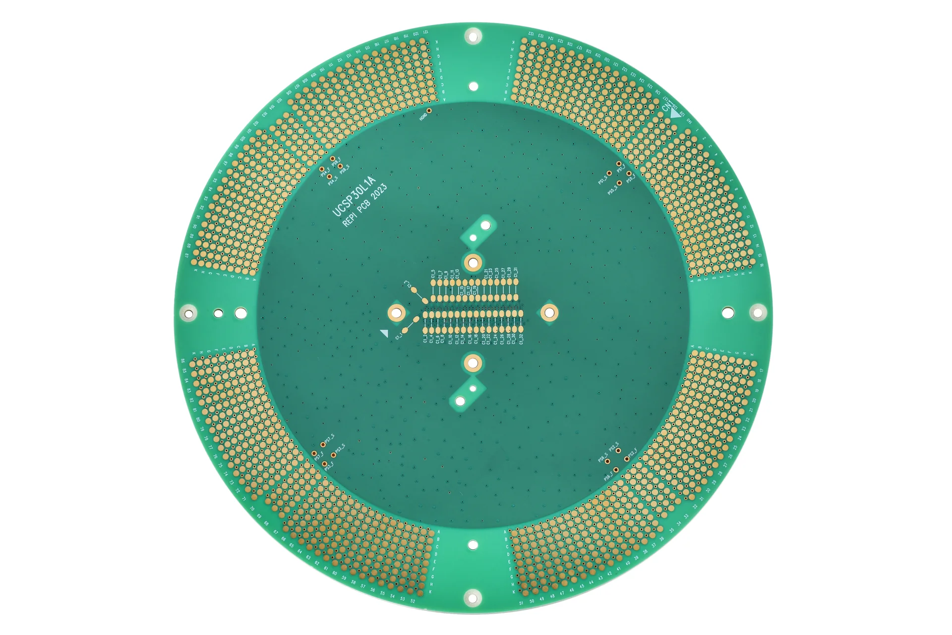
Multilayer test PCB showing the outline, mounting holes and pad pattern. It is not a power-supply layout example or a test result.
The board outline must also appear in the fabrication profile. For CNC-routed edges, define the contour, slots and internal cutouts clearly, and keep mounting holes consistent with the board outline and enclosure. The image below shows an outer-profile routing process. It illustrates a CNC fixture and panel, not a specific outline or machining parameter for this article. 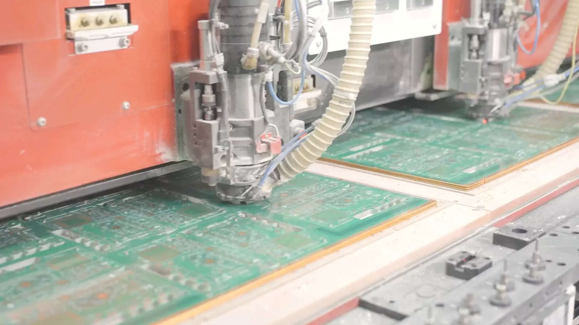
CNC profile-routing process, showing the cutter, machine table and PCB panel. It is not a power-board example or a machining-capability claim.
For an overview of board types used in power electronics, see KnownPCB's energy and power electronics PCB category. Confirm the outline, mounting locations and component heights against the project's mechanical drawing.
In an isolated flyback or forward supply, the transformer is both a power component and the physical boundary between the primary and secondary sides. Use the actual transformer outline, pin numbers, winding assignments and insulation requirements to define a keepout area. Place primary-side and secondary-side parts on their respective sides of that boundary. Do not estimate safety spacing from the transformer body alone. Pins, pads, copper layers and the path across the board surface all affect creepage and clearance.
The primary side usually includes the input filter and bulk capacitor, switching MOSFET, primary current sense and the power-related part of the controller circuit. The secondary side includes the output rectifier, output capacitors and load connector. If the design uses an optocoupler, its position must also follow the isolator data sheet and applicable safety standard. Do not route other parts, copper or planes across the isolation boundary for convenience.
Isolation spacing depends on working voltage, insulation class, pollution degree, material and the applicable standard. A transformer withstand rating does not guarantee that PCB copper spacing is adequate. Check board-edge paths, slots and component pins separately. TI's flyback reference design states that the PCB spacing between its high-voltage primary and low-voltage secondary must meet the applicable safety requirements. The project standard and product conditions determine the actual dimensions.
Place the primary MOSFET near the transformer primary pins and the related input capacitor. Do not let a connector, control trace or mounting hole force the current path to detour. If the current-sense resistor, gate resistor and driver belong to the same switching stage, position them near the MOSFET according to the controller's reference layout. In TI's TIDA-01505 flyback reference design, the input film capacitor, SiC MOSFET and current-sense resistors sit close to the transformer to shorten that design's main current loop. Use this relationship as a layout reference. Do not copy its board layers, part numbers or dimensions.
Place the input bulk capacitor near the primary supply entry and switching stage so its forward connection and ground return are clear. A high-frequency bypass capacitor serves a different location. Follow the controller's pin-layout guidance and keep that capacitor near the relevant supply pins. If all capacitors are grouped at the input connector, the switching device may still have a long path to its local bypass capacitor.
The MOSFET and transformer area also produces heat. Leave room for a heatsink, insulating pad, mounting screw and airflow. Check that these mechanical parts do not intrude on the isolation boundary. If the device pad needs thermal vias, confirm the package drawing, via type and fabricator capability before placing them. Do not apply one via count to every design without a stackup. KnownPCB's article on high-current PCB via fabrication and DFM provides additional manufacturing context.
Place the secondary rectifier diode or synchronous rectifier MOSFET near the matching transformer secondary pins. Leave room for its pad, copper area and heat path. The first ceramic capacitor should sit close to the rectifier and output return so current does not travel through another area before reaching the capacitor. Place the bulk output capacitor and connector along the load path, while keeping output return current out of the primary-side reference area.
Capacitor size and temperature also affect placement. Check the height, polarity and temperature limits of an electrolytic capacitor. Do not place it against a hot transformer or rectifier. A small ceramic capacitor can sit closer to the rectification node. A bulk capacitor also needs room for its body, mounting and service access. ST's PM8803 layout note places the rectifier near the transformer's output side and separates the first and final ceramic capacitors. That guidance applies to its PoE controller reference layout.
If power devices or capacitors need larger copper areas to conduct heat, see KnownPCB's heavy copper PCB category. Select copper weight, pad area and thermal-via structure for the device losses, stackup and fabrication capability. The category page does not establish a thermal design.
Place the input connector, primary switching stage, transformer, secondary rectifier, output capacitor and output connector in the order that power moves through them. Then check where each trace enters and leaves. Do not route the input through the secondary-side small-signal area, or send the output trace back across the primary side to reach its connector. Give sensing and control lines a separate exit path away from the transformer, switch and rectifier.
Feedback and current-sense networks are more sensitive to switching noise than the power copper. Keep their parts near the controller pins they serve. Connect sense points as the schematic specifies, and separate the sense traces from gate drive, switch nodes and rectifier current paths. Do not split a ground plane only because the schematic uses the names "analog ground" and "power ground." Use the current-return path and controller guidance to decide how the board should be partitioned.
Hot components need room too. The MOSFET, transformer and rectifier can sit near their own power paths without being packed together so tightly that they block airflow or heatsink mounting. If the enclosure acts as a heat spreader, coordinate the component location with its contact surface, insulating pad and clamp. Keep temperature-sensitive feedback parts and electrolytic capacitors away from local hot spots, within their stated temperature limits.
The fabrication drawings should identify the board outline, mounting holes, slots, copper layers, solder-mask openings and transformer keepout. The copper gap between primary and secondary, the path around the board edge and the layer arrangement must agree across the stackup and output files. A silkscreen label that says "high-voltage area" does not establish isolation. Fabricator-approved drill, plugging and copper-weight notes must refer to the same revision as the PCB files.
Compare each library footprint with the actual transformer, MOSFET, rectifier and capacitor model. Check pin numbers, pad dimensions, component height and polarity. Similar-looking transformers can have different pin maps and isolation-slot locations, so do not substitute a footprint based on appearance alone. Before release, check hole-to-copper, copper-to-edge, pad-to-mask and safety-region rules. Ask the fabricator to confirm special holes, edge slots and heavy-copper features can be made as drawn. These checks cover the board geometry and fabrication requirements, not placement or soldering instructions.
TI's TIDA-01505 reference design shows component placement on a specific wide-input flyback board and discusses primary-to-secondary isolation. ST's AN3387 for the PM8803 PoE controller gives relative placement guidance for input capacitors, switching parts, rectifiers and output capacitors. TI's Fly-Buck isolation guidance says creepage and clearance must follow the chosen isolation grade and safety standard. The three references cover different topologies and applications. Their dimensions are not universal rules.
For a review of the board outline, stackup or special holes, send the schematic, full fabrication files and mechanical drawing to the KnownPCB engineering team. Mark the primary-to-secondary boundary, critical footprints and fixed mounting points.
Not by default. Set the board outline, connectors, mounting holes, isolation boundary and transformer footprint first. Then place primary- and secondary-side parts around their paths. The center, edge or heatsink area is not a universal location. Check winding sides, enclosure space and safety spacing.
No. Working voltage, insulation class, material, pollution degree, product standard and the path across the board surface all affect creepage and clearance. The electrical-safety requirements for the product must set the target, and the layout and fabrication files must show it.
The output capacitor should be near the rectifier path, but it also needs separation from local heat sources. Set candidate positions from the electrical path, then check capacitor temperature limits, height, cooling and enclosure space. Do not lengthen the return path just to move the capacitor farther away.
TI's TIDA-01505 flyback reference design layout guide shows the main-loop component placement and discusses PCB safety spacing between its high- and low-voltage sides.
ST's AN3387 PM8803 layout application note describes relative placement for the transformer input capacitors, primary switching parts, secondary rectifier and output capacitors.
TI's Fly-Buck isolation-boundary and creepage guidance says transformer-side creepage and clearance must follow the isolation grade and applicable safety standard.
October/10/2026DC-DC Converter PCB Layout: Paths, Thermal Vias and Noise
April/15/2026Why Stackup Is the Starting Point of a Manufacturable HDI Board
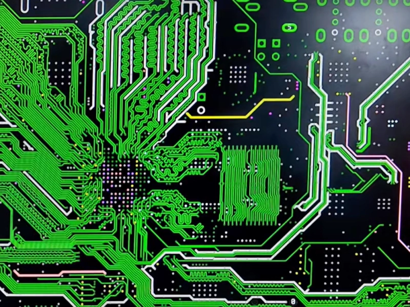
May/13/20268 Layer PCB Manufacturing and DFM Guide
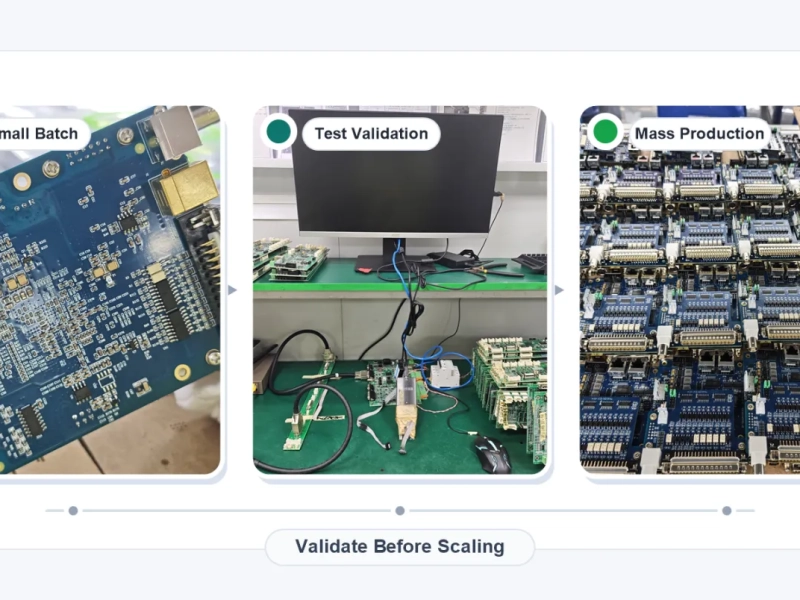
July/23/2026PCB Common DFM Mistakes and Solutions
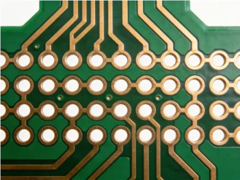
September/14/2026High-Current PCB Via Manufacturing: DFM, Plating & Reliability
 | Download our design guidesfor better PCB designing and manufacturing These are some of the design guides designers and engineersdownload the most:
|
Proven by 7 industries, 4000+ customer projects
Please contact us at sales@knownpcb.com, ask for engineering support here or use the form below to reach out to KnownPCB | Get In Touch Today |