Blog & Design Guide

DC-DC converter PCB layout starts with the current path in each switching state. The paths in a buck converter differ from those in a boost converter, so placing the switch, magnetic component and capacitors close together is not enough. A poor return path can put the feedback trace or switching node in a noisy area. This article focuses on layout and fabrication-file checks. It does not replace the controller data sheet or component design.
KnownPCB's power supply PCB page shows related board types. It is not a converter design example. The layout notes below follow the topologies and constraints described in the cited references.
Table of contents
Before laying out the PCB, mark the current loops for the switch's on and off states on the schematic. Use separate colors for continuous current, rapidly changing current and small-signal feedback. The drawing does not need trace-width calculations. It needs to show where current leaves, which parts it passes through and where it returns. Then place these paths over the preliminary board outline and check whether connectors, mounting holes or component footprints occupy critical loop areas.
In a common buck converter, when the high-side switch is on, current flows from the input capacitor through the high-side switch and inductor to the output, then returns to the input capacitor through ground. When the high-side switch turns off, the inductor continues to supply the load. The return current flows through the low-side MOSFET, or through the freewheel diode in a nonsynchronous design. Keep the fast input commutation loop between the input capacitor and the high-side/low-side switch pair, or diode, compact. Check the output current loop separately. The output capacitor's positive terminal connects to the inductor output, and its return path connects to the low-side switch or freewheel diode. These loops serve different purposes. An output capacitor near the connector does not prove that either path is correct.
In a boost converter, the inductor is usually in series with the input. When the switch is on, input current flows through the inductor and MOSFET to ground. The output rectifier is off, so the output capacitor supplies the load. When the switch turns off, inductor current flows through the rectifier diode or synchronous rectifier to the output capacitor and load, then returns to the input side. Place the input capacitor near the point where input current enters the switching stage. Place the output capacitor near the rectifier and its return. These parts belong to different current paths, so a buck arrangement cannot be copied directly. TI's boost converter layout guide identifies the fast loop formed by the MOSFET, rectifier and output capacitor. Check the actual controller topology before using a reference layout.
Start with constraints outside the circuit. Fix the input and output connectors, board outline, screw holes, heat-sink contact areas and enclosure keepouts. Then place the power switch, inductor or transformer, rectifier and input and output capacitors. Each time a part moves, check whether its current path has lengthened, its return has been interrupted or the feedback network has moved next to a switching node.
Place capacitors according to the current they carry. The input ceramic capacitor connects between the input supply and power ground, so it should sit near the controller or external switch supply pins. The output capacitor follows the inductor and rectifier output path, with a short positive connection and ground return. A bulk capacitor can support lower-frequency energy changes, but it does not replace the high-frequency bypass capacitor near the switching stage. Follow the controller manufacturer's pin-layout guidance when you set the final positions.
For a board with larger copper areas or multilayer connections, see KnownPCB's energy and power electronics PCB category. A product category does not define the stackup or electrical drawing. Select the layers, copper weight and via structure for the project.
When a power trace moves from the surface to an inner layer, check more than electrical continuity. High-frequency current returns through a nearby reference plane. A slot, plane split or distant return via can enlarge the actual loop. At each layer transition, confirm that the reference plane remains continuous, a nearby return connection is available and the vias do not violate clearance to adjacent nets. If the trace can stay on one layer and keep the loop shorter, frequent layer changes do not help.
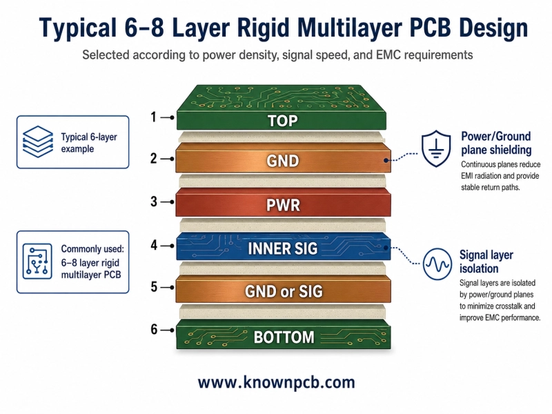
Do not choose a via count from current alone or copy a generic drawing. Stackup, finished-hole diameter, copper plating, copper width, frequency and temperature-rise limits all affect the result. Multiple vias can lower the impedance between layers and spread heat. They can also cut a continuous return plane or crowd the copper around a pad. Treat the via positions, via type and connecting copper as one geometry when you check a parallel connection.
For a high-current layer connection, KnownPCB's article on high-current PCB via fabrication and DFM can help you compare the design goal with fabricable via structures, plating and stackup conditions. Its manufacturing discussion does not guarantee the current capacity of a particular design.
The exposed pad on a controller, a power MOSFET pad or a rectifier copper area may conduct heat. Thermal vias carry heat from the device layer to an inner layer or the other side of the board. They also occupy pad area and affect soldering and fabrication. Check the package drawing first to see which pads allow vias. Then set the via field using the stackup thickness, copper weight, hole capability, solder-mask definition and any fill requirement. Do not use a universal via count or pitch without the package and stackup details. 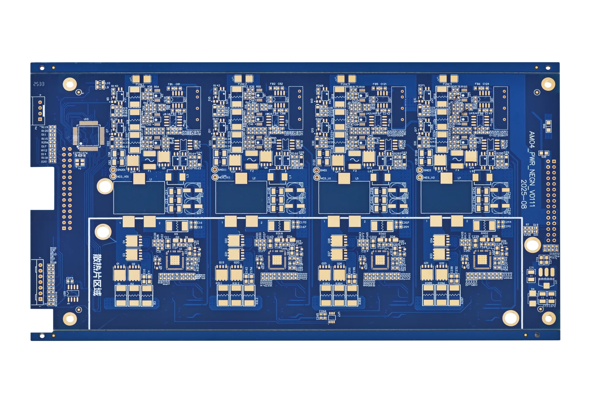
Multilayer heavy-copper PCB panel showing copper areas and mounting holes. It is not a DC-DC converter example or an EMI test result.
Connect the hot-area copper to an inner plane or bottom-side copper, then check whether the neck is too narrow, the plane is split or nearby nets need electrical isolation. If power ground also carries switching return current, do not enlarge the switch-node copper just to gain heat-spreading area. ROHM's step-down layout application note discusses power-ground area, adjacent ground planes and via placement. Its specific recommendations apply to the circuit conditions in that note.
KnownPCB's heavy copper PCB page describes the product category. Heavy copper does not replace thermal vias or automatically solve switching noise. Specify copper weight, trace width and via structure in the stackup and fabrication data.
The SW node changes voltage quickly between switching states. The MOSFET gate drive and rectifier area can also carry rapidly changing voltage or current. Keep the feedback divider, compensation network and enable signal away from these areas. Do not run them parallel to the SW trace for a long distance or under the inductor. Connect the feedback sense point where the controller documentation specifies. If the design uses remote sensing, route the sense line separately from the load point rather than picking it up anywhere along a high-current output plane.
A quiet area does not require isolated ground islands. Keep power return current on the planned path and give small signals a continuous, clear reference plane. Check whether a feedback trace crosses a plane split. If it does, adjust the stackup or component placement before adding a reference via. TI's buck converter layout note and ROHM's EMC guide discuss how the current loops, switching nodes and sensitive signals relate in a layout.
Before sending the board for fabrication, check that the stackup, copper layers, drill files and solder mask describe the same board. If thermal vias must be plugged, capped or left open, state that in the relevant layer data and fabrication notes. Check the relationship between copper and via lands against the hole size and finished-hole capability agreed with the fabricator. A via under a component pad also needs to match the pad definition and soldering requirements. Electrical continuity alone does not make the drawing complete.
Then check the board outline, mounting holes, keepouts, copper-to-edge spacing, layer clearances and isolated copper. If the project uses heavy copper, blind or buried vias, or special hole processing, make sure the stackup and drill notes use the same revision. Resolve undefined via types and conflicting solder-mask requirements in the CAM feedback. Fabrication data must state the design intent; a generic current-carrying formula cannot replace a review of the actual structure.
The fabrication files and process photos describe different stages. The process image below shows a PCB held in an electrical test fixture. It only shows the fixture and board position. It is not a DC-DC converter example or evidence of EMI, load or operating-performance results. 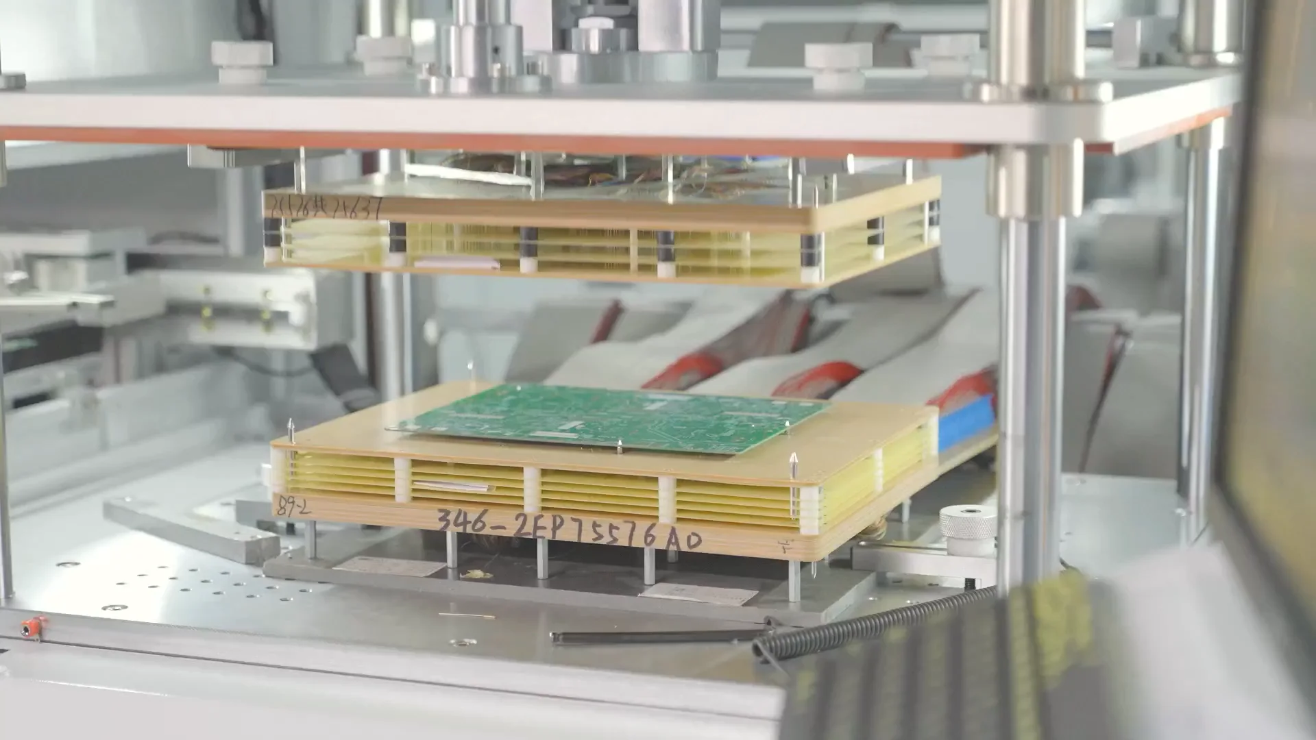
PCB electrical test fixture, showing the board between the upper and lower fixtures. It does not show EMI or operating-performance validation of the layout discussed here.
ROHM's step-down DC-DC layout and EMC application note covers input capacitors, power ground, adjacent ground planes, vias and feedback routing. Apply its recommendations only to circuits with matching conditions.
TI's TPS61022 and TPS61023 boost layout guidelines show the current paths during the on and off states of a boost converter and discuss the relationship between the MOSFET, rectifier and output capacitor.
TI's buck-converter layout application note discusses the input hot loop, output current loop and layout parasitics. Check its recommendations against the actual buck structure.
If you need to review a stackup, via structure or fabrication layer, send the schematic, complete fabrication files and mechanical drawing to the KnownPCB engineering team. Mark the thermal pads, layer transitions and via-treatment requirements. Electrical and thermal conclusions still depend on the component data and test results.
They can share checks for the board outline, stackup, feedback isolation and fabrication files. Draw the current paths between input capacitors, switches, rectifiers and output capacitors separately for each topology. The boost inductor and output rectifier loop do not follow the buck capacitor order.
No single value fits every board. The pad, package thermal resistance, stackup, copper weight, finished-hole capability and soldering requirements all affect the layout. Start with the component documentation, then confirm via diameter, pitch, fill and solder-mask details with the fabricator.
Yes, but check the return path and parasitic inductance on both sides of the transition. A via that forces fast return current to detour can make the layout worse. Keep the main commutation path short and continuous. If it must change layers, review the power via, reference-plane connection and nearby return via together.
 | Download our design guidesfor better PCB designing and manufacturing These are some of the design guides designers and engineersdownload the most:
|
Proven by 7 industries, 4000+ customer projects
Please contact us at sales@knownpcb.com, ask for engineering support here or use the form below to reach out to KnownPCB | Get In Touch Today |