Blog & Design Guide

Fast switching currents on an SMPS PCB create magnetic fields and can couple noise into nearby nets through parasitic inductance and capacitance. A layout review should identify the paths with rapidly changing current, check whether the return follows the forward path, and look for noise coupling into sensitive signals.
This article covers common board-level checks for switched-mode power supplies, with a focus on hot loops, return paths, and EMI risk. It is limited to bare-board DFM and layout context. It does not develop a specific DC-DC topology's input and output paths, thermal design, or feedback network, and it does not claim to replace system EMI verification or certification.
Table of contents
A hot loop is a closed path whose current switches rapidly or changes sharply as the power switch changes state. It is not a name for every DC current path on the supply board. Each topology has different paths, so a Buck example cannot be copied directly to a flyback, boost, or resonant supply.
When the switch changes state, current in some conductors changes in magnitude or direction. Parasitic inductance turns that change into voltage spikes, and a larger loop area makes magnetic coupling into nearby conductors more likely. Making the copper wider does not compensate for an unnecessarily long loop or a return path that detours.
Start with the schematic. Mark the current direction during the on and off states, then identify the segment that carries current in only one state or changes rapidly. Analog Devices' article on switched-mode power-supply layout also compares switch states to identify critical current paths. After identifying the path, mark its component pads, copper, and return area on the PCB.
ADI's AN-139 application note on power-supply layout and EMI treats rapidly changing current loops as a major source of radiated noise and discusses how loop area and parasitic inductance affect the field. The review should protect the fastest-changing closed path first, then arrange the remaining nets. It does not need to crowd every component together.
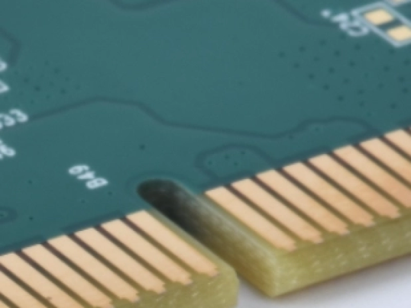
The photo below shows pads and copper on a multilayer bare board. It is not an SMPS layout and does not mark a hot loop.
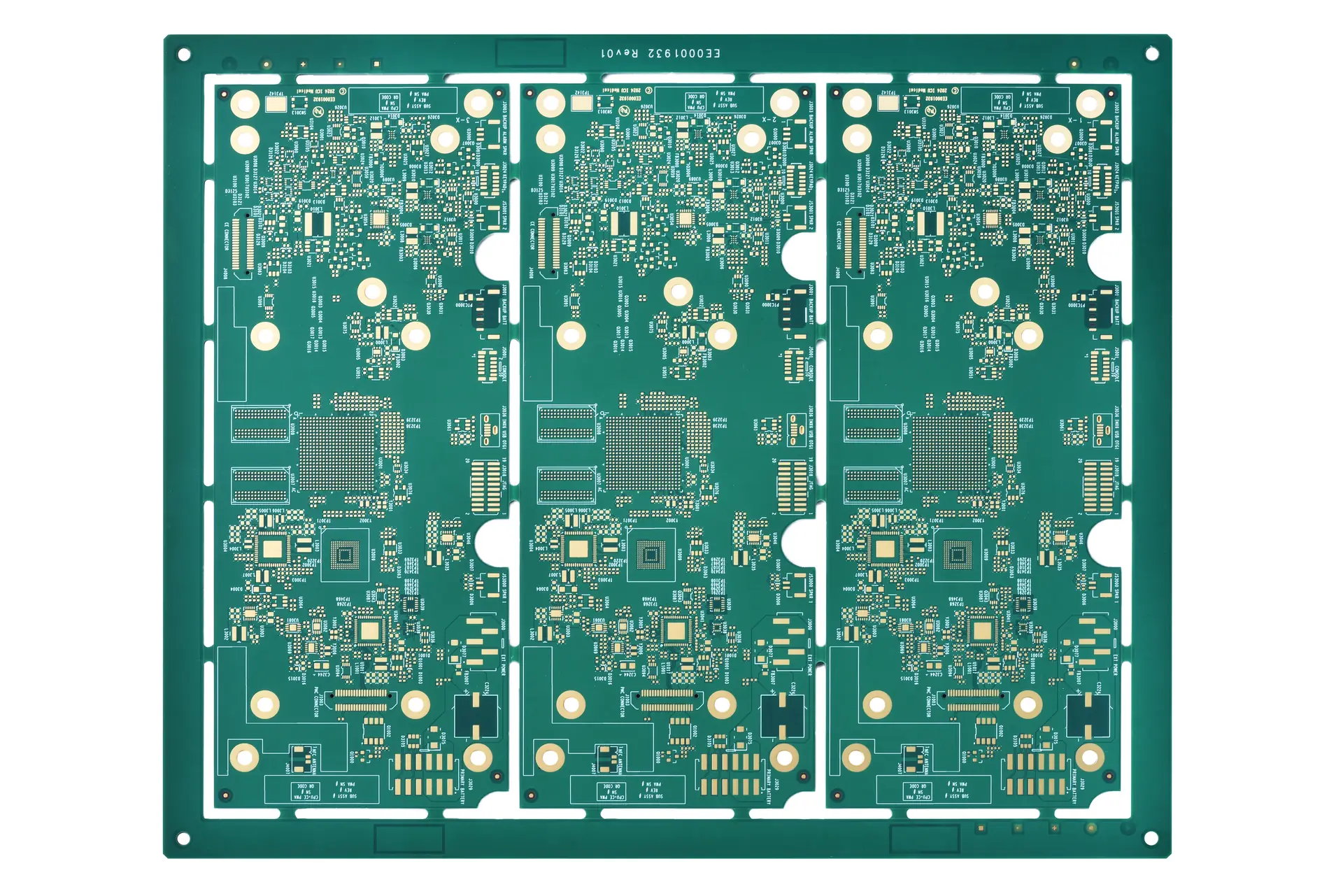
Multilayer bare-board panel. The photo does not show an SMPS topology or EMI test result.
Current must flow in a closed loop. High-frequency return current tends to follow a path with lower impedance, but it does not necessarily travel in a straight line along the ground symbol in the schematic. For each forward-current segment, find the adjacent reference plane or copper return, then check for splits, slots, non-ground vias, or connector pads that interrupt it.
When a top-layer forward trace sits close to a continuous inner-layer return plane, the pair can form a smaller loop. If a slot or plane split cuts off the reference path, current may detour elsewhere, increasing the loop area and magnetic field. On a multilayer board, inspect the copper layer by layer rather than relying on the component side alone.
Grounding cannot be reduced to "always split power and signal grounds" or "always keep one solid plane." Confirm the schematic connections, isolation boundaries, and current paths first. Then check how the plane carries return current. Any plane split needs a clear electrical reason, and the design should not force fast or pulsed current to detour.
If several high di/dt loops share a narrow copper neck, via, or return segment, record it. Shared impedance lets voltage changes from one loop appear in another and can create ground bounce or coupled noise. The review sheet should identify the shared segment and affected control nets instead of saying only "the ground trace is too long."
A switching node can carry both a fast voltage transition and pulsed current. A large copper area at that node increases parasitic capacitance and can couple noise into nearby ground, a chassis, or sensitive signals. The board review should check the copper shape and its extensions across layers, then consider whether any high di/dt copper can be reduced without compromising the current and thermal requirements of the device.
Do not route sensitive control, measurement, or communication nets parallel to a switching node. If the layout cannot avoid the crossing, review their overlap on different layers, the dielectric separation, and the reference planes between them. TI's power-supply PCB layout seminar materials identify switching-noise coupling, filter returns, plane continuity, and test setup as review points.
If the input and output sides of an EMI filter run parallel for a long distance on the board, noise may couple around the filter. Check that the paths from the connector to the filter and from the filter into the power area remain separated. Confirm that filter ground and chassis connections follow the circuit and component requirements. The schematic alone cannot show whether the filter works as intended in the layout.
When reviewing EMI, separate the noise source, coupling path, and affected net. The source is often a fast switching voltage or current. Coupling may occur through shared copper impedance, magnetic fields, parasitic capacitance, or filter routing. The affected net is a control or measurement signal that must remain stable. This structure makes the review note specific instead of labeling the design only as "EMI risk."
Magnetic coupling can also occur between high-frequency transformers or inductors. A board review can check their orientation, spacing, and proximity to low-level nets near high di/dt nodes. The detailed placement of magnetic components and winding shields depends on the magnetics and topology; this article does not prescribe one placement template.
Vias change the geometry of both forward and return paths. When current changes layers, check that the forward connection and its reference-layer connection are both available. Also inspect the return plane for non-reference vias, slots, and copper gaps. Mark each layer transition on the review plot when a current path crosses multiple layers.
In a Gerber or ODB++ viewer, display power copper, ground planes, switching nets, and sensitive nets separately. Trace the outgoing and return paths on the same annotated view. A visible ground plane does not prove that the return path is continuous. Layer transitions, plane splits, and copper near the board edge are common places to miss.
If a high-current path uses several parallel vias, review the via copper, drill size, and connecting copper area against the order requirements. KnownPCB's high-current via article covers via structure and plating DFM. It does not replace hot-loop or EMI layout review.
A board-level DFM review needs enough context. Provide the schematic, complete Gerber or ODB++ files, stackup, finished thickness, copper weight, drill files, and board outline. Identify the hot loops and important return areas. With Gerber files alone, a fabricator can inspect copper geometry and manufacturing rules, but cannot reliably identify each net's function or which copper carries rapidly switching current.
A reviewable checklist can record the on/off current paths on the schematic, the matching PCB locations, return-plane continuity, switching copper that extends across layers, filter paths that may be bypassed by adjacent nets, and topology assumptions that still need confirmation. Include each file revision and layer name so a later revision can be compared at the same locations.
EMI failures can come from the circuit, cables, enclosure, and final installation. Bare-board DFM can identify a detour, an unnecessarily large copper area, or a broken plane, but it cannot prove that a product passes conducted or radiated emissions testing. Test reports need to identify the sample, operating mode, cable setup, and test conditions.
If the project uses near-field scanning or a pre-compliance EMI scan, record probe position, scan height, operating mode, and cable setup. Before-and-after measurements can show the effect of a layout change only when the conditions are comparable. A pre-scan is not the same as formal testing under the target product standard.
ADI's board-layout article and TI's power-supply PCB materials both recommend reviewing switching current, return paths, and noise-sensitive areas together. KnownPCB's power supply PCB page and energy and power electronics page describe related board categories. The quality management page provides inspection context. To review Gerber files, the stackup, and return-path structures, contact the KnownPCB engineering team for bare-board DFM.
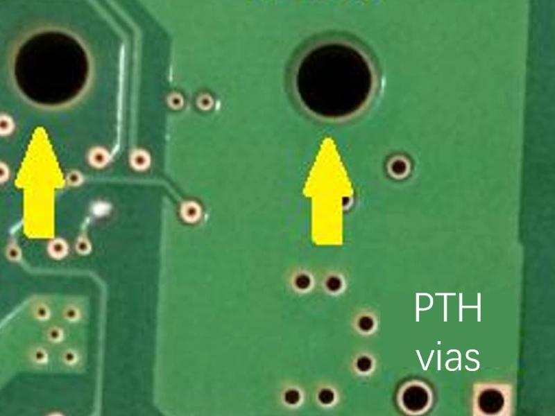
The second photo shows pads and copper on a multilayer PCB. It helps illustrate board features that may appear in a layer review, but it is not an SMPS schematic and does not indicate current direction.
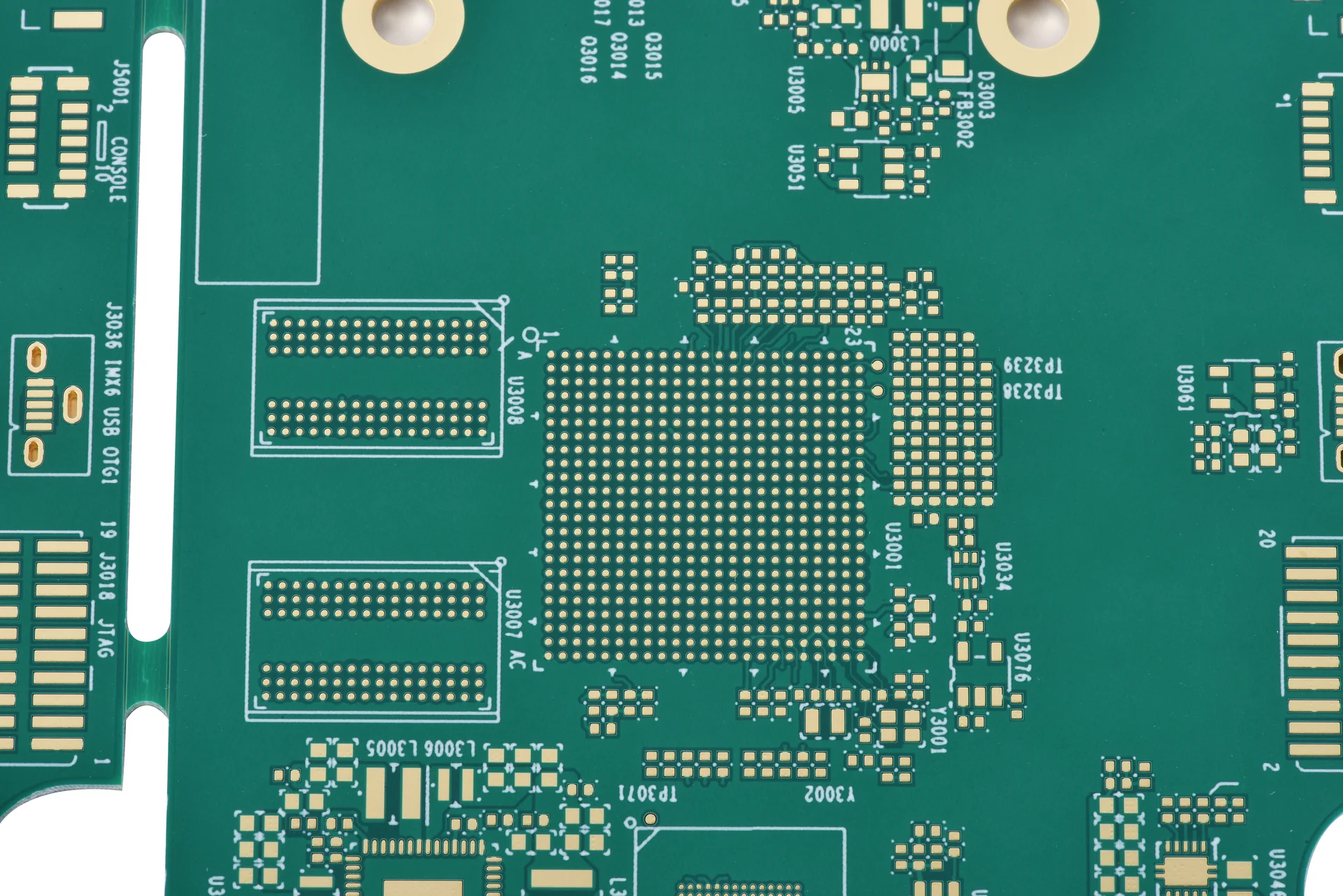
Multilayer bare-board detail. The photo does not show an SMPS hot loop or EMI performance.
It is a closed path where current changes rapidly as the switch changes state. Identify it by comparing the actual schematic in the on and off states. Look for segments that conduct in only one state or whose current changes sharply. The hot loops differ by topology.
There is no fixed answer for every switching supply. Check the net connections, isolation boundaries, and actual return paths. An arbitrary plane split can force current to detour; connecting separate grounds without following the circuit can also break isolation or increase noise.
No. DFM can inspect copper geometry, return planes, switching-net spacing, and fabrication features. It cannot replace conducted or radiated testing on the assembled product. The result depends on the circuit, cables, enclosure, and test setup.
Analog Devices, AN-139: Power Supply Layout and EMI.
Analog Devices, The Golden Rule of Board Layout for Switched-Mode Power Supplies.
 | Download our design guidesfor better PCB designing and manufacturing These are some of the design guides designers and engineersdownload the most:
|
Proven by 7 industries, 4000+ customer projects
Please contact us at sales@knownpcb.com, ask for engineering support here or use the form below to reach out to KnownPCB | Get In Touch Today |