Get A Quote
CN
Blog & Design Guide

Via-in-pad solves a layout problem by putting a via inside a component land. VIPPO adds a filled via and a plated copper surface over it. Those words describe more than a via location. The drawing must also identify the layer span, fill, cap, finish, and acceptance plan that the supplier is being asked to build.
This guide reads the structure from the solderable surface down to the target layer, then turns that cross-section into a fabrication note. It keeps routing choices separate from process limits. No fill material, copper-cap thickness, or surface-flatness value should be assumed without agreement for the actual construction.
Begin with the package land map and the intended layer transitions. A conventional dog-bone fanout moves a short trace from the component pad to a nearby via. Via-in-pad places the via in the pad instead. This can free a crowded breakout area, but it also puts a plated hole structure directly under a soldered component terminal.
Use the structure where the routing or thermal path needs it. A board does not gain anything from putting every via inside a land when ordinary fanout already fits. A via under a BGA signal ball and a via under a QFN thermal land also have different solder and heat-flow roles, so review them as separate cases.
On the layout, mark the exact pads that need via-in-pad treatment. Identify the package, pad number, destination layer, and whether the connection is a signal, power, ground, or thermal path. Keep ordinary vias in the same footprint group clearly distinguishable. This stops an open via near a component from being mistaken for a filled-and-capped one.
In this article
A VIPPO cross-section is easiest to read from the component-facing surface down. It shows the solderable land, the copper that closes the via opening, the material inside the hole, the plated barrel, and the target land at the end of the layer span. The drawing should identify which layers the via connects. A top-view Gerber alone does not show the fill or the buried connection.
| Cross-section feature | What it does | What the drawing should identify |
|---|---|---|
| Surface finish | Provides the final solderable surface over the land. | The selected finish and which surfaces receive it. |
| Copper cap | Covers the filled opening and restores a continuous copper land. | The via group and whether one or both sides are capped. |
| Fill material | Occupies the via cavity beneath the cap. | The agreed fill type and locations. |
| Barrel plating and target land | Connect the component-side land to the destination layer. | The start layer, stop layer, hole family, and destination land. |
These parts are related but they are not interchangeable. The finish is not the copper cap, and a resin-filled hole is not automatically a plated-over land. A cross-section drawing should also distinguish a through via from a blind microvia. The start and stop layers determine how the board is built and which copper interfaces need review.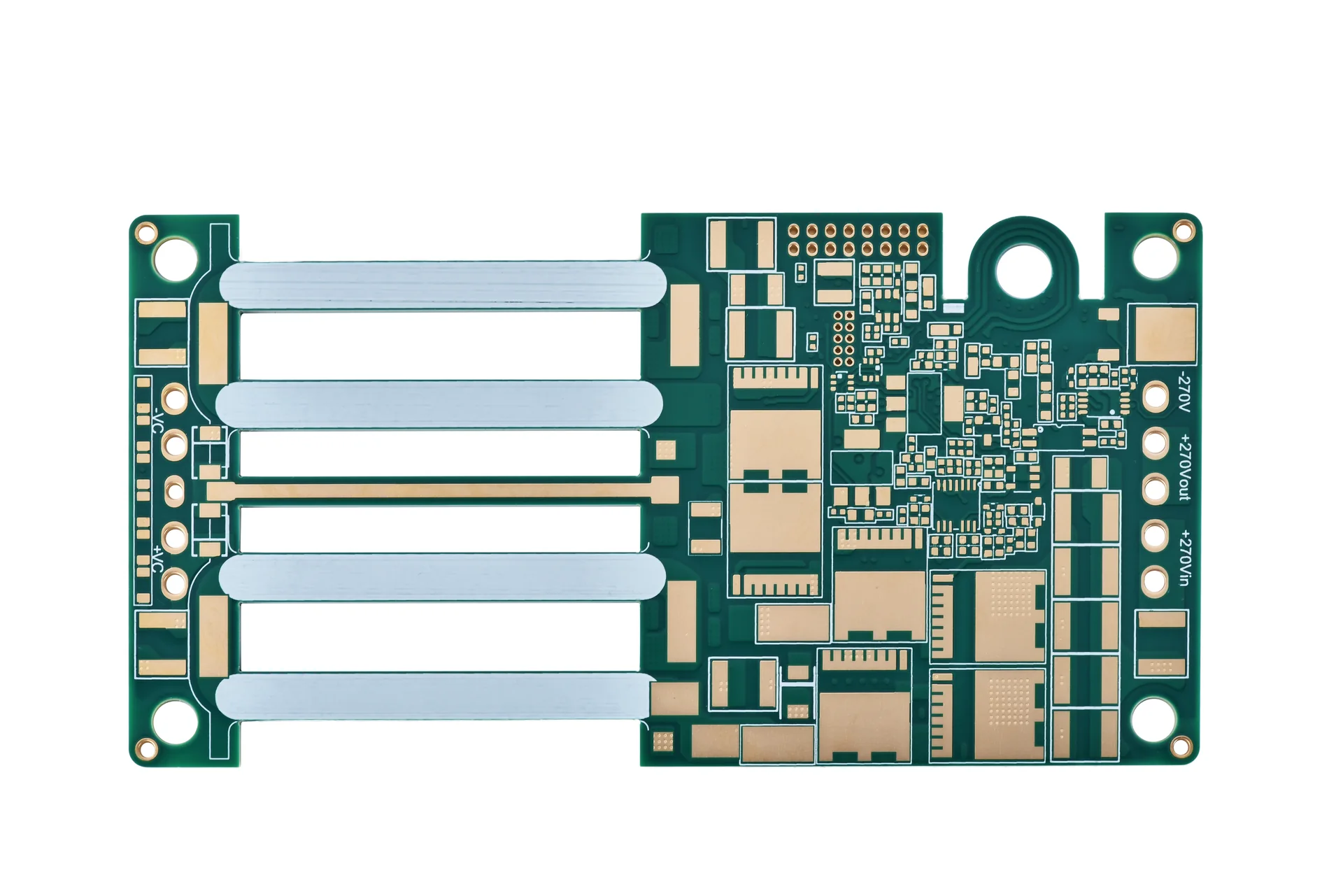
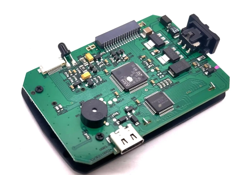
A top-side product view shows via-in-pad lands but does not reveal the internal fill or copper-cap cross-section.
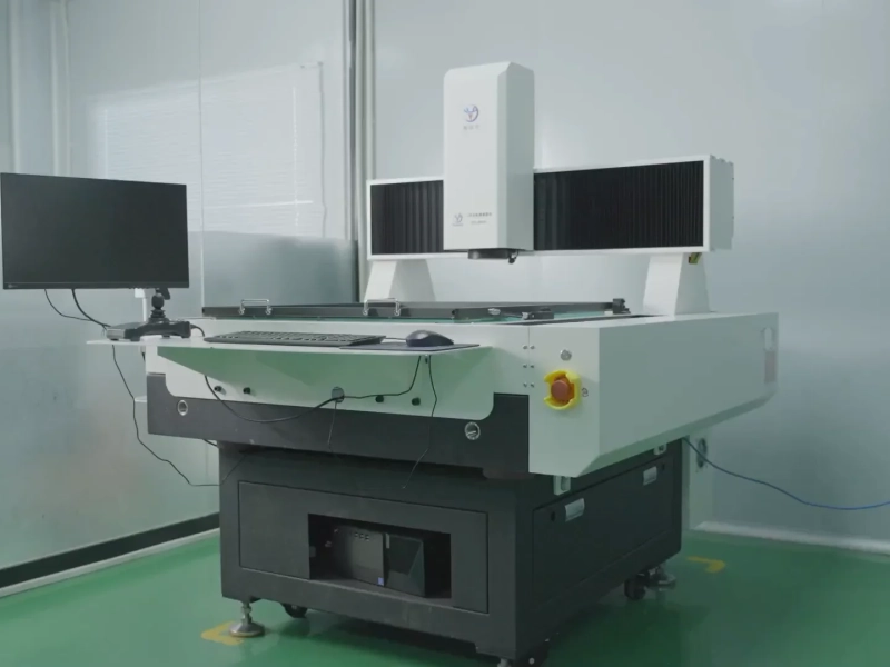
A common VIPPO route forms and plates the via, fills the remaining cavity, stabilizes the fill, removes excess material from the surface, and plates copper across the opening. The final surface finish is applied to the land. The order and exact process depend on the via type and the supplier’s qualified construction, so the drawing should specify the result the project needs rather than assume one universal sequence. The photo below shows resin-hole plugging equipment as one process step; it does not show a completed VIPPO cap or cross-section.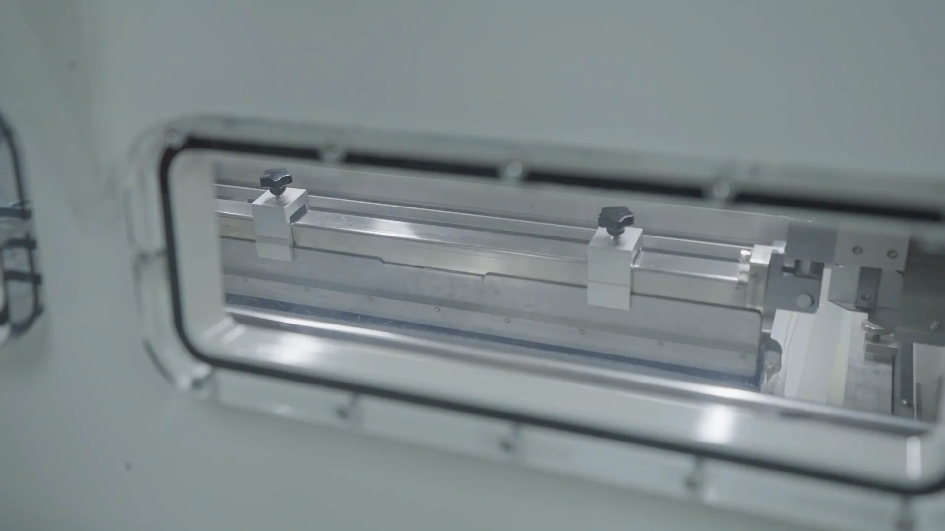
Resin via plugging is shown as a process step; this image is not a VIPPO cross-section or a copper-cap inspection record.
Fill material can be resin or a conductive material such as copper. The choice affects the structure and must follow the electrical or thermal design intent. A conductive fill is not automatically a better design, and a nonconductive fill does not remove the electrical path because the plated barrel and cap carry the connection. State the fill type in the fabrication notes when the design depends on it.
Planarization removes excess fill so the next copper surface can form the intended land. The cap then closes the filled via from the component side. A recessed fill, raised bump, incomplete cap, or poor interface can affect the land and solder joint. Those are inspection concerns to agree with the supplier, not dimensions to copy from another board design.
The IPC-4761 via-protection guide lists Type VII as a filled-and-capped via structure and separately covers planarity and via metallization. Use the type name only when it matches the construction being requested. It does not set a universal fill material, cap thickness, or surface-flatness tolerance for every VIPPO design.
Put the pad and via in the same package drawing review. Confirm the component land pattern, the via location within the pad, the finished hole definition, and the annular copper that remains after registration and plating. For a blind or laser microvia, identify the capture layer and target layer. For a through via, identify that it crosses the full board. Do not let a generic label hide the actual layer span.
Check the pad’s surrounding mask opening, copper clearance, neighboring lands, and routed escape. The via may fit on the top view yet collide with an inner-layer trace or with another via transition. Include the stackup and the relevant copper layers when asking for a manufacturability review.
KnownPCB’s HDI capability reference lists via-in-pad, resin plugging, copper filling, and electroplated fill for higher-level HDI. The HDI PCB capability page gives the broader product scope. A project still needs agreement on its specific layer pair, fill, cap, and acceptance criteria.
Use a via map, drill table, stackup, and fabrication note that point to the same locations. Identify which vias require filling and capping, their layer spans, and the pad or net reference that distinguishes them from ordinary vias. If only selected BGA rows use VIPPO, mark those rows rather than applying the note to every via in the footprint area.
State whether fill and cap are required on one side or both sides. Name the material if the application depends on it. Identify the surface finish, and provide the acceptance method for any important planarity, void, cap, or interface requirement. If the project has no approved numerical value, ask the fabricator to propose a limit and record the approved response. Do not leave a value to CAM interpretation or copy a number from a different board thickness and layer span.
Send the released Gerber or other agreed manufacturing data with the drill files, layer stackup, fabrication drawing, and revision. The CAM review should identify any conflict between the component pad, via location, mask opening, and via-treatment note. If the supplier proposes moving a via or changing the fill, return the changed layer view for engineering approval before the revision is released.
A useful review checks the structure that the drawing asks for. Confirm the intended layer transition, inspect the fill and cap on an agreed sample or coupon when required, and compare the resulting surface with the approved acceptance plan. An electrical continuity check alone does not show whether the cap, fill, or surface matches the drawing.
KnownPCB’s quality management overview describes inspection and test resources. For a project-level discussion, share the stackup, via map, package land pattern, and fabrication note through KnownPCB’s contact page. These files let the engineering review focus on the actual structure, not on a single word such as VIPPO.
February/26/2026PCB Warpage: CTE Mismatch, Asymmetric Stack-Ups, Copper Imbalance and Reflow Control
February/03/2026Type of PCB Edge Connectors Overiew

February/26/2026HASL vs ENIG vs Hard Gold: Cost, Solderability, Flatness and Wear Resistance
October/10/2026Power Supply PCB Creepage and Clearance: DFM Review
April/14/2026Features of PCB for Industrial application
Proven by 7 industries, 4000+ customer projects
|
Please contact us at sales@knownpcb.com, ask for engineering support here or use the form below to reach out to KnownPCB |
Request a Manufacturing QuoteInclude your quantity, target delivery date and key requirements. File handling and NDA information. |