Get A Quote
CN
Blog & Design Guide

Stacked and staggered microvias solve different routing constraints. A stacked path keeps successive vias on the same vertical axis. A staggered path shifts each transition on an intermediate layer and joins the lands with copper. The choice changes the available surface area and the interfaces that need review, so it should follow the actual layer transition rather than a universal pitch rule.
Start with the net that has the least room to escape. Mark its component pad, destination layer, nearby lands, and the routing channels available between them. A staggered path needs room for an intermediate land and copper segment. A stacked path uses less surface area at the transition. Ball pitch alone does not require one arrangement.
Both structures can connect the same layer pair. The top view shows alignment or offset, while the cross-section shows each hole’s start and stop layers and the support below the next transition. Review the copper path and the local return path together because a lateral offset changes where the connection turns between layers.
This article compares those layout choices with the manufacturing drawing. It treats reliability as evidence about a specific construction and test, not as a fixed multiplier attached to the word “stacked” or “staggered.”
In this article
| Review question | Stacked path | Staggered path |
|---|---|---|
| Where do the vias land? | On the same vertical axis across successive layer pairs. | At offset positions connected through an intermediate copper feature. |
| What does the layout need? | Less lateral routing area at the via transition. | Room for the offset lands and the connecting route. |
| What should the fabricator review? | Layer-to-layer registration and the support, fill, and surface of stacked interfaces. | Offset, land clearance, the intermediate copper path, and registration. |
| What does the name prove? | Only the arrangement, not a reliability result. | Only the arrangement, not a reliability result. |
Test the offset route against the actual pad geometry and clearances. If the intermediate land collides with a neighboring pad or blocks another connection, record that collision. Then compare a stacked path for that location.
Keep the electrical path visible. A moved connection can change where copper turns between layers and alter the local reference-plane transition. Check both the outgoing route and its return path in the same layout.
A stacked arrangement often needs additional preparation between build-up steps so the next via lands on a defined copper surface. A staggered route may need more room and an extra copper connection. The exact fill and plating requirements depend on the layer pair, via type, materials, and stackup. Do not assume that every staggered via is unfilled or that every stacked via uses the same fill process.
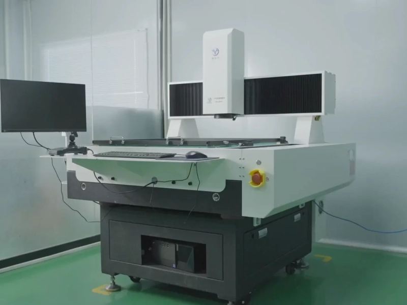
Keep each microvia’s depth and diameter separate from the layout choice. Moving a via sideways does not change the hole’s aspect ratio. The approved stackup and supplier rules should define the geometry for each via family. The photo below shows laser drilling equipment, not the geometry or reliability of the depicted vias.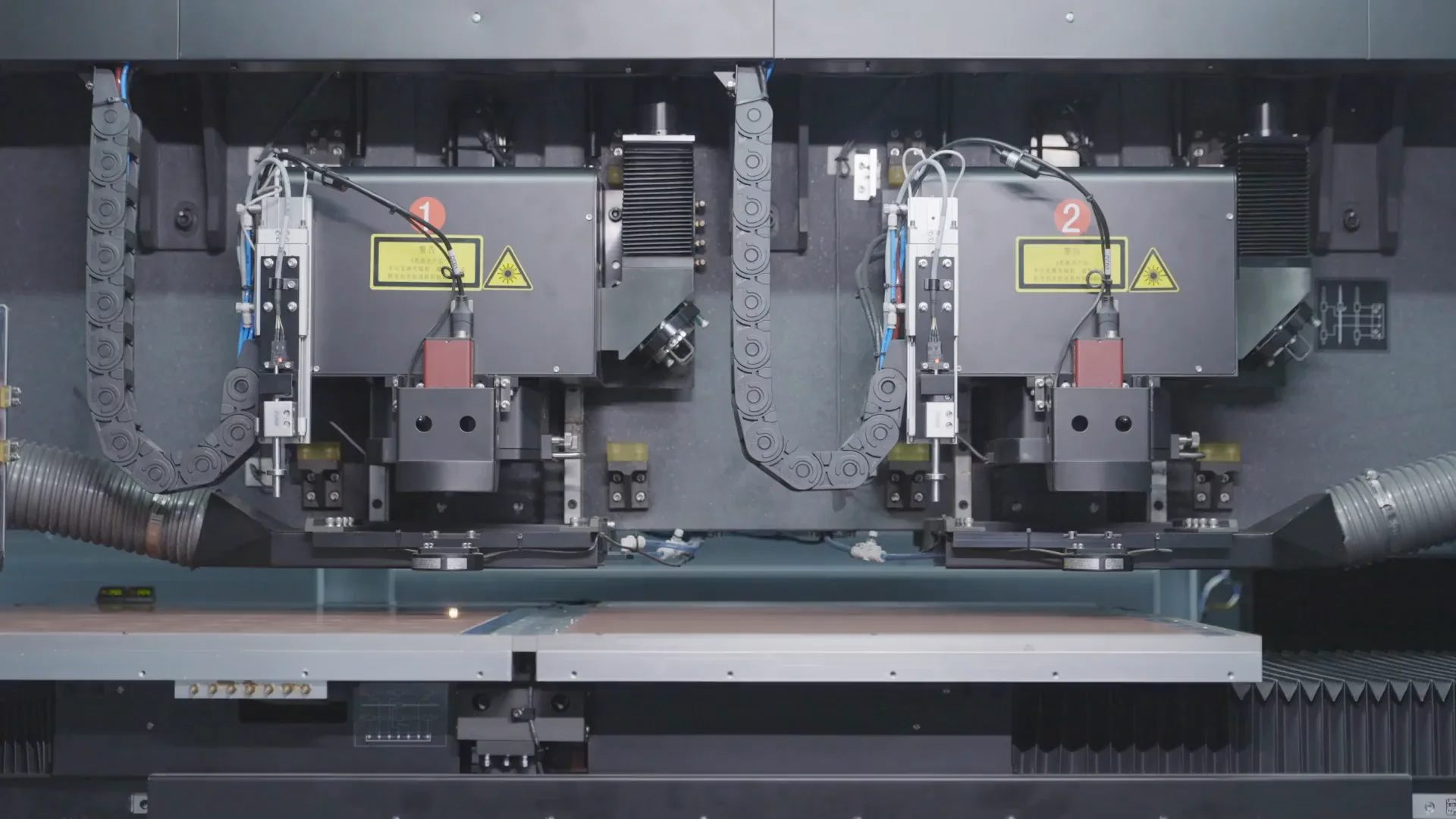
Laser drilling equipment is shown as process context; this image is not a stacked or staggered microvia cross-section.
Reliability belongs to the complete construction, not its label. The relevant details include the number of via levels, the support below the stack, the laminate and copper, fill and cap details, layer registration, and the assembly or field stresses the board must pass. A study of one coupon does not set a universal pass rate for a different board.
An IPC technical paper on microvia design and reliability compares stacked and staggered connections under its own coupon and thermal-test conditions. The paper reports that the tested structures did not perform identically. Its result supports checking the proposed structure and test plan; it does not provide a fixed reliability multiplier for every stacked or staggered design.
When reviewing a supplier test report, keep the sample construction, material, via map, thermal profile, acceptance criterion, and sample count beside the result. Ask whether the report tested the same number of via transitions and the same support below the microvias as the proposed board. Without those details, “passed” does not tell the layout team which structure was actually demonstrated.
The HDI microvia cracking analysis article covers defect investigation separately. Use that type of failure analysis when the concern is an observed crack or separation. A routing comparison should not claim to diagnose a defect from the via arrangement alone.
A board can use both patterns. A constrained group of inner BGA signals may need a stacked route, while nearby connections can take an offset path if there is enough copper space. This avoids expanding the most demanding construction to every net without a layout reason.
Mixed routing still needs a consistent drawing. Identify each via family and its start and stop layers. Mark which paths stack, which paths offset, and where the intermediate connection lands. Show fill or cap requirements where the structure calls for them. A general note such as “stack where required” leaves the CAM reviewer to decide which nets are allowed to change.
Review the net path after any offset is added. Check the connecting trace, clearance to other lands, reference plane changes, and any sensitive signal requirement. If a proposed fabrication change moves a via or changes the connecting layer, compare the revised path with the approved layout before release.
A useful review package includes the stackup, layer-pair drawing, via map, land dimensions, and notes for the fill and cap treatment. Show the full path from the component-side capture land to the target layer. Include the materials and the expected inspection or reliability evidence when they are part of the product requirement.
KnownPCB’s HDI capability reference lists stacked and staggered microvias among supported HDI structures. The HDI PCB capability page gives the broader product scope. The exact layer count, support structure, and verification plan still need review for the board being quoted.
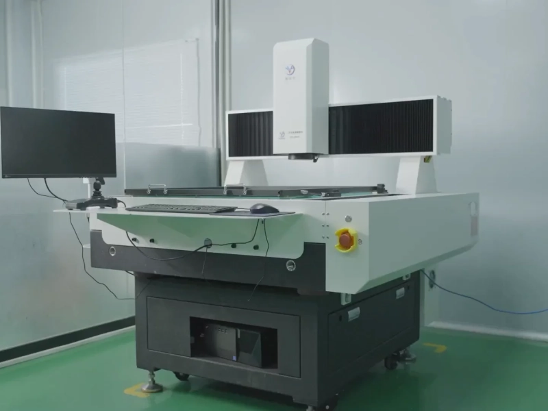
The photo below shows X-ray drill targeting equipment. It is a manufacturing process image, not a layer-registration measurement for a particular stack. For a project review, send the stackup and via map through KnownPCB’s contact page so the team can review the stated transition and fabrication notes.
X-ray drill targeting equipment is shown as process context, not as a layer-registration measurement or reliability result.
February/25/2026High-Frequency PCB Performance: Low Dk/Df, Controlled Impedance and Low Signal Loss
February/03/2026Type of PCB Edge Connectors Overiew
February/26/2026PCB Via Protection Types
October/15/2026Microvia Aspect Ratio: Measure Depth and Diameter
October/10/2026DC-DC Converter PCB Layout: Paths, Thermal Vias and Noise
Proven by 7 industries, 4000+ customer projects
|
Please contact us at sales@knownpcb.com, ask for engineering support here or use the form below to reach out to KnownPCB |
Request a Manufacturing QuoteInclude your quantity, target delivery date and key requirements. File handling and NDA information. |