Blog & Design Guide

Microvia aspect ratio compares the depth of one microvia with a specified hole diameter. The result is useful only when the drawing names the layer span, the depth datum, and the diameter used in the calculation. A tapered laser via has a larger opening at its capture side and a smaller opening at its target side, so an unlabeled diameter can produce different answers for the same feature.
This guide sets out a calculation method and a hypothetical example. It keeps microvia geometry separate from plated-through-hole ratios. The board’s total thickness is not the depth of a single blind microvia.
In this article
First identify the structure. A laser microvia usually connects a capture layer to a target layer below it. A blind via may span a different layer pair, and a skip via may cross more than one dielectric layer. Record the starting and ending copper layers so the team can tell which hole is being discussed.
For a tapered hole, name both ends. The capture-side opening is the entrance at the layer where the microvia starts. The target-side opening is where it terminates. Those are hole diameters. The copper capture land and target land are separate pad diameters and should not be substituted for the hole openings in the ratio.
Use consistent units for depth and diameter. If the drawing gives the dielectric thickness, the outer copper foil thickness, or both, state which dimensions contribute to the depth value. Published design references do not always present the same drawing convention in the same way. A clear note lets the layout team and fabricator compare the same geometry.
The basic calculation is:
Aspect ratio = defined microvia depth ÷ defined hole diameter
Call the numerator H and the chosen diameter Dref. Then calculate H divided by Dref. Do not use the pad or land diameter as Dref unless a project standard explicitly defines it that way. Do not substitute overall PCB thickness when the hole connects only a short layer pair.
One published Altium microvia-sizing reference writes the ratio using the outer dielectric thickness plus outer copper foil divided by microvia diameter. Treat that as one documented convention. The project drawing should still state the applicable standard, layer pair, copper inclusion, and diameter datum. IPC lists IPC-2226 as its HDI printed-board design standard; use the revision named in the product requirements rather than relying on an old excerpt or an unlabeled calculator.
For each via family, the drawing should make it possible to answer three questions without interpretation: where does the hole start, where does it stop, and which diameter is used in the ratio? Record the capture-side opening and target-side opening even when the calculation uses only one of them. This makes a later drill or stackup change easier to compare.
A microvia ratio uses the depth of its own layer transition. For a blind microvia, use the span between its capture and target layers according to the agreed drawing convention. For a skip via, include the full span that the laser-formed structure crosses. For a stacked connection, calculate each microvia level separately. Do not divide the full stacked path by one hole diameter unless the controlling specification explicitly defines a combined ratio.
This is different from a plated-through-hole ratio, where the drilled barrel may cross most or all of the finished board. A thick-board PTH rule cannot be copied onto a laser microvia. The KnownPCB capability snapshot lists PTH aspect-ratio values that conflict across general and HDI references; that row does not establish a microvia limit.
Stackup changes can alter H after routing begins. A thicker dielectric or a change to the intended target layer changes the depth term. If the hole diameter stays fixed, the calculated ratio changes as well. Recalculate each affected via family whenever the material, layer span, or copper construction changes.
Consider a hypothetical blind microvia with a defined depth of 70 μm, a 100 μm capture-side opening, and an 80 μm target-side opening. These are example dimensions for explaining the calculation. They do not describe a KnownPCB capability or a production recommendation.
| Calculation input | Value in this example | Meaning |
|---|---|---|
| Defined depth H | 70 μm | The layer-pair depth under the stated convention. |
| Capture-side opening | 100 μm | The wider entrance diameter in this tapered example. |
| Target-side opening | 80 μm | The narrower termination diameter in this tapered example. |
If the project defines the capture-side opening as Dref, the calculation is 70 ÷ 100, or 0.70:1. If it defines the target-side opening as Dref, the calculation is 70 ÷ 80, or 0.875:1. The hole has not changed. Only the denominator changed.
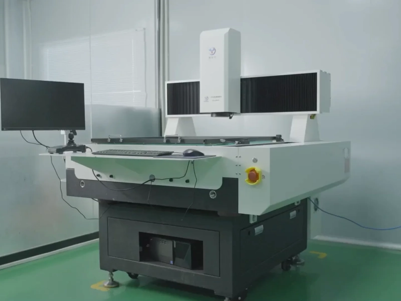
That difference is why the ratio on a drawing should include its datum. The example does not decide which convention a particular fabricator or specification uses. Ask the fabricator to confirm the definition and use the same one in the drill table, stackup, DRC rule, and acceptance record. The photo below shows laser drilling equipment used in microvia formation; it does not show a measurement for this example.
Laser drilling equipment is shown as process context; the photo does not show a microvia diameter or depth measurement.
Do not leave the fabricator to infer the microvia geometry from a pad stack or a shaded 3D view. Put the dimensions and layer span in the controlled fabrication package. A drill table and cross-section callout should agree with the top-view Gerber or other manufacturing data.
For each via family, identify:
When a cross-section drawing shows a tapered profile, label the wide and narrow sides. If dimensions are finished sizes rather than as-drilled sizes, say so. Keep the hole opening, plated barrel, capture land, and target land in separate callouts. One unlabeled “via diameter” can refer to several different features.
The image below shows a drilling inspection screen. It is an equipment view, not a microvia cross-section or a measurement for the hypothetical example.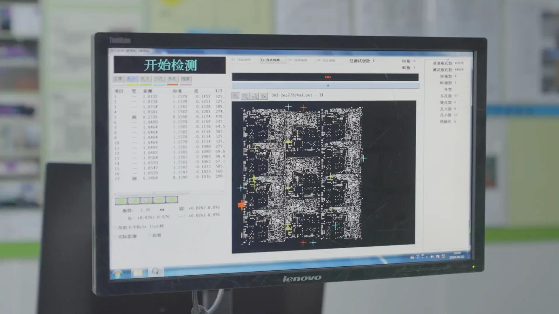
A drilling inspection screen is shown as process context, not as a microvia aspect-ratio measurement.
Set the stackup before freezing the BGA fanout. Confirm each dielectric layer, the target layer, and the drilled or finished opening convention with the fabricator. Then calculate the ratio for every different layer pair. A single board can contain more than one microvia family with different depths or tapers.
KnownPCB’s public HDI capability table lists laser-hole diameters and microvia aspect-ratio fields by build stage. Check the row that matches the actual 1-step, 2-step, 3-step, or any-layer construction, then confirm the material and layer span with engineering. The HDI PCB capability page gives the broader product scope.
For background on HDI construction, see the HDI board introduction. For a project review, send the stackup, via table, and drawing through KnownPCB’s contact page. Confirm the ratio convention before routing is released, then keep the approved dimensions with the drawing revision.
October/14/2026HDI PCB Solder Mask: Fixing Fine-Pitch Gerber Issues
July/03/2026Single Sided PCB Board: How to Design and Purchase

September/06/2026High Current PCB Design: Current Paths, Copper, Vias & Thermal Limits
March/30/2026The Definition of Through Via, Blind Via, Buried Via
September/14/2026High-Current PCB Via Manufacturing: DFM, Plating & Reliability
Proven by 7 industries, 4000+ customer projects
Please contact us at sales@knownpcb.com, ask for engineering support here or use the form below to reach out to KnownPCB | Request a Manufacturing QuoteInclude your quantity, target delivery date and key requirements. File handling and NDA information. |