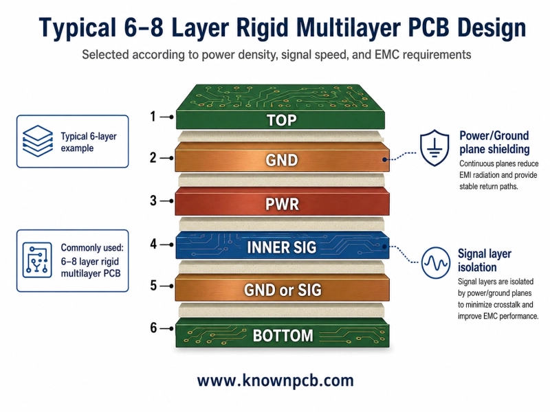

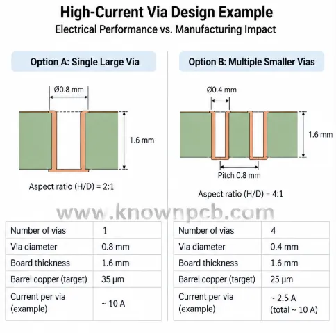
There is a gap between Nominal Model and Fabrication Reality. While high-current PCB engineers model vias as ideal cylinders in EDA simulations (e.g., Altium, Ansys), high-current PCB factories produce non-uniform, tolerance-bound structures through drilling, desmear, and electroplating—all subject to drilling and plating limits.
This article focuses on fabrication, plating and repeatability. If you first need to determine via diameter, barrel copper thickness, via count, current sharing and temperature rise, start with our High-Current PCB Via Design Guide.
How Does PCB Via Aspect Ratio Affect Plating Distribution for High-Current PCB?
Aspect Ratio = PCB Thickness / Drill Diameter
Let’s see the example, it is with a 2.0 mm board and a 0.30 mm drill:
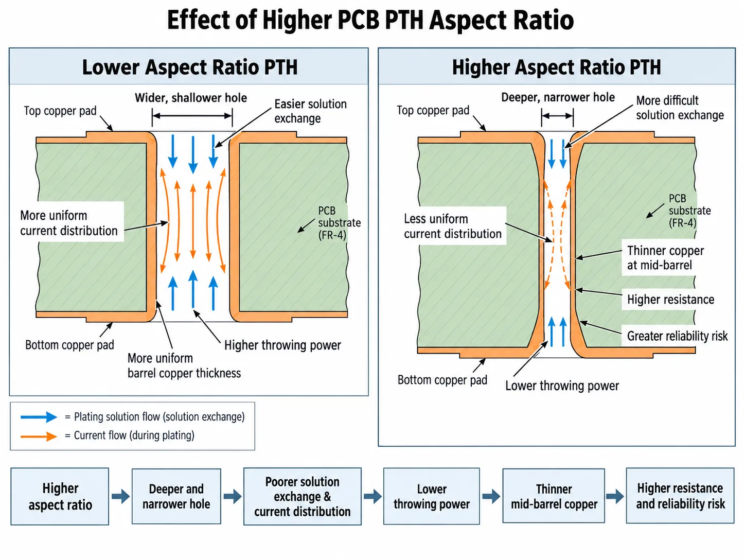
The real manufacturing challenge is often plating it uniformly. We can more easily understand why the depth-to-diameter relationship affects copper distribution during plating.
Here is schematic diagram about Aspect Ratio and Plating Distribution
For high-current boards that also require increased conductor thickness, see KnownPCB Heavy Copper PCB manufacturing capabilities. Via geometry, finished hole copper, surface copper build-up and outer-layer processing should be considered together rather than as independent specifications.
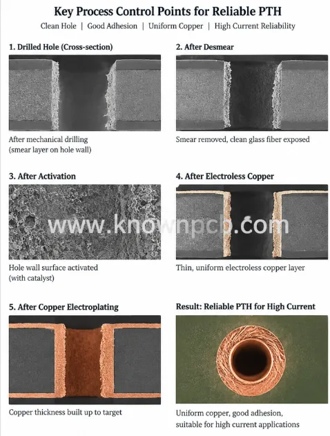
How Is a High-Current PCB Plated Through Hole Manufactured?
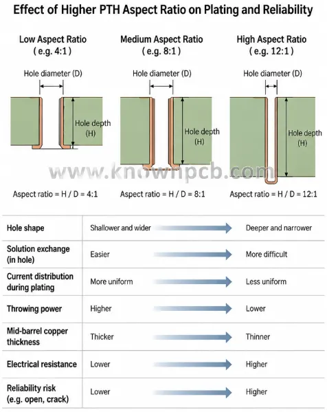
Why Does Higher Aspect Ratio Make PCB Via Plating More Difficult?
A deep and narrow hole is more difficult to plate. As the aspect Ratio increases, throwing power goes down.
Why Are Design Value, Process Target and Measured Value Different?
Design Value
We suppose the electrical design uses a barrel copper thickness of 25 μm in its resistance calculation. The high-current PCB design model may implicitly picture the barrel as having 25 μm of copper everywhere.
As we all know, Real plating is not perfectly uniform, so the finished hole can have thicker and thinner regions.
Process Target
Let’s see the process target.
The high-current PCB process target may need to be different from the nominal design value, depending on the fabricator’s process window.
Measured Value
The actual result obtained from the finished board, for example through microsection measurement. You will find that copper thickness varies significantly along the barrel wall once you cut it open (PCB Cross-sectioning)
Minimum local copper thickness can matter because local conductive area decreases where the copper is thinner, thus the average barrel copper thickness is not a full picture.
J(x) = I / A(x)
The manufacturing window starts with the electrical design requirement. For the relationship between via diameter, barrel copper thickness, resistance, via count and temperature rise, see our High-Current PCB Via Design Guide.
Does Manufacturable Mean Repeatably Manufacturable for a High-Current PCB?
Manufacturable is also not stable or repeated orders or High-current PCB.
Assume a fabricator publishes the following capability limits:
- Minimum drill = 0.20 mm
- Maximum aspect ratio = 8:1
Your high-current PCB design is :
The next theme is about stable manufacturing of high-current PCB.
We evaluate a high-current PCB manufacturer by their capabilities, but it will not be a guarantee of high-current performance at repeated orders. The lot-to-lot consistency in high-current applications is driven by a moving cocktail of bath chemistry, drill wear, and base material variations.
For a 30 A via array, the high-current PCB designer factor in the following points:
| High-Current Via Array Factor | Manufacturing / Performance Concern |
|---|---|
| Copper distribution | Copper thickness is not perfectly uniform throughout the via barrel. |
| Local resistance | Local barrel geometry affects conductive area and resistance. |
| Current sharing | Via-array geometry and copper paths influence current distribution. |
| Temperature rise | Resistance and heat spreading determine local thermal performance. |
| Process variation | Drilling and plating variations affect finished via geometry. |
| Lot-to-lot stability | Repeat production must maintain a controlled process window. |
Via manufacturing is only one part of the complete power path. For trace width, copper thickness, layer transitions, connectors, current crowding and thermal limits, see our High Current PCB Design Guide.
What Happens When Barrel Copper Increases from 25 μm to 50 μm?
Increasing Barrel Copper from 25 μm to 50 μm
If we keep the drill size and high-current PCB board thickness the same, moving from 25 μm to 50 μm copper doubles the cross-section and theoretically cuts the resistance in half.
If it is a must-have adjustment, high-current PCB factory reconsider:
- the target copper thickness
- whether the minimum copper thickness can be maintained along the hole
- how barrel plating interacts with surface copper build-up
- whether subsequent outer-layer processing remains inside a stable process window.
What does this mean for the high-current PCB project? The PCB factory will recheck the cost, delivery time etc.
Is it really worth driving up outer-layer complexity and cost across the whole board just to shave a fraction of a milliohm off the via resistance?
We compare increasing hole copper, adding more vias, changing via diameter, optimizing via-array position, or improving current spreading in the top and bottom copper planes.
If the project requires more conductor cross-section, increasing barrel copper is only one option. Compare the via strategy with Heavy Copper PCB manufacturing before increasing plating requirements across the entire board.
Pushing for a heavier hole-copper spec, the high-current PCB designer forces a much deeper review of the fab's process window:
- Plating capability
- Copper-thickness uniformity
- Surface copper build-up
- Outer-layer line/space processing
- Cost and yield
Why Must High-Current PCB Design and Manufacturing Form a Closed Loop?
Conclusion: Design and Manufacturing Form a Closed Loop
The high-current PCB specification directly affect PCB manufacturing.
At the same time, the hole geometry and copper structure of high-current PCB that the PCB factory can reproduce consistently determine whether the original high-current PCB design calculation remains valid.
The full engineering relationship between high-current PCB design and PCB factory can therefore be summarized as:
What Should You Confirm Before Releasing a High-Current PCB?
Before releasing a high-current PCB, confirm:
- What is the target hole copper thickness?
- What is the guaranteed minimum local hole copper?
- What aspect ratio is inside the stable production window?
- How is hole copper verified?
- Is the value a capability limit or a standard production capability?
- How is lot-to-lot consistency controlled?
Move From a Nominal Via Design to a Manufacturable High-Current PCB
Send KnownPCB your board thickness, finished hole size, target barrel copper, current requirement, Gerber files, and production volume. Our engineering team can review the via structure together with plating capability and repeat-production requirements.
Request DFM Review Explore Industry SolutionsHigh Current PCB Design: Current Paths, Copper, Vias & Thermal Limits
High-Current PCB Via Design: Current Capacity, Via Size & Via Arrays
References
IPC-6012F — Qualification and Performance Specification for Rigid Printed Boards
IPC-2221B — Generic Standard on Printed Board Design
Altium — PCB Via Aspect Ratios and Their Importance in Multilayer PCBs
18-year sale engineering experience in PCB industry. A versatile sales engineer with both engineering background and international project experience. She is familiar with HDI, high-speed boards and small-to-medium batch manufacturing requirements. Being capable of quickly understanding the design pain points of customers and providing a one-stop PCB solution from DFM to mass production.