Blog & Design Guide

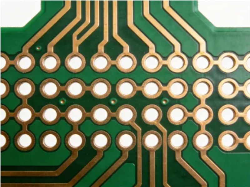
A single-sided PCB has a clear routing constraint: every electrical net must connect on one copper face. The challenge is not only connecting every pad. Crossovers, return paths, power routes, and fabrication clearances also need room. Fix the board outline and critical components first, use jumpers only for crossings that cannot be routed around, and review each important current path. This article covers bare-board routing. It does not give a universal trace width that ignores current, copper thickness, or fabricator capability.
Table of contents
Before routing, confirm that the schematic and netlist match. In the PCB tool, restrict signal routing to the intended copper face. Mounting holes, locating holes, and non-plated holes do not provide an electrical connection between copper layers. Each net must either connect fully on the copper face or use a jumper that is clearly specified in the design data.
The KiCad PCB Editor documentation describes copper layers, nets, track widths, and design rules. Remove unused copper layers from the routing choices and define clear rules for each net class. This reduces the chance of routing onto the wrong face. A design-rule check can find unconnected nets and width or clearance violations. It cannot decide whether the return path is sound or prove that a trace can carry the required current.
When checking the netlist, review the power input, ground, connectors, test points, and protection devices first. If a connector pin or circuit function has changed, update the schematic and netlist before routing again. This avoids moving components to fit an outdated netlist, only to find a missing or misconnected net later.
Group components by circuit function, then set the fixed board boundaries. Place external connectors, mounting holes, edge keepouts, and parts with orientation constraints first. Next place devices with many pins or dense connections, and leave clear channels from their pins to nearby circuit blocks. Route according to the circuit relationships, not just to make the components look aligned.
On a single-sided layout, rotating one component can determine whether several nets can pass between its pads. Before routing, check the footprint pads, component spacing, and the direction in which nearby nets leave each footprint. If a connector or package blocks a group of signals, try changing its orientation or position before adding jumpers.
Leave continuous space for copper and return networks. If a ground connection reaches the main ground through only a narrow neck, a load current may share that copper with a sensitive signal. Sketching the critical loops during placement is easier to review than trying to add ground paths after every signal has been routed.
When traces cross on a single copper face, first change the net route or component placement. Use a jumper wire or zero-ohm resistor only when the crossing cannot be avoided. Give each jumper pad a clear net name, footprint, orientation, and location that can be inspected. A jumper does not create a copper connection through the bare board. It is a separate connection that needs to be documented.
Review each crossover: do both ends connect to the intended nets, is there clearance from nearby pads and the board edge, and could the jumper obstruct another part or test point? If a route must cross several important signals, or jumpers force power and ground paths to detour, go back to placement and routing order or compare a double-sided layout. There is no jumper-count limit that fits every circuit. The relevant question is whether the jumper changes the electrical path or complicates the manufacturing data.
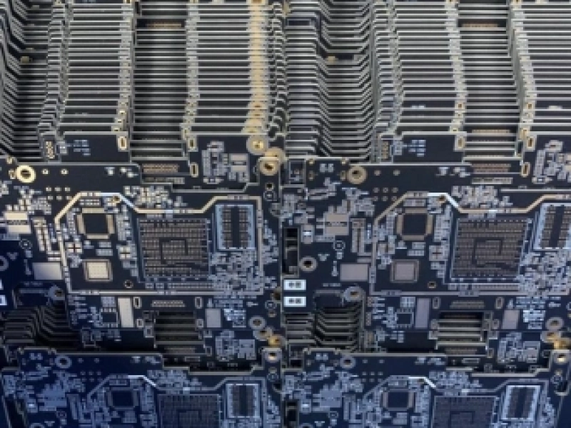
The outer-layer etching photo shows a production line carrying PCB panels through process equipment. Etching is one step used to form copper patterns. This equipment photo is not a single-sided routing diagram and does not prove that a netlist or return path is correct.
PCB outer-layer DES etching line. The equipment photo does not show a single-sided layout or an etching measurement result.
Every signal has a return-current path to its source. For faster signals, return current concentrates near the trace in the reference conductor. A slot, break, or narrow neck in that copper can force the return path to detour and enlarge the loop. TI's Practical PCB Design Rules explains how a slot in the reference plane can divert return current and increase loop area.
A single-sided board has no separate internal ground plane, so do not copy a multilayer-board copper-pour assumption. Check whether ground copper has become isolated islands, whether it connects to the main ground through narrow necks, and whether important signals have a usable return path nearby. If signal traces and ground copper share one face, inspect the actual gaps after the copper pour is filled. Keep or remove isolated copper according to its net and the manufacturing data.
For high-current paths such as power, motors, or switching nodes, trace the complete supply-and-return loop. Check whether it passes through sensitive analog ground or a connector reference. For clocks, communications, and other fast-edge signals, reconsider the single-sided structure if there is no continuous reference path. A wide ground trace does not guarantee that high-speed return current stays close to the signal.
If power ground and small-signal ground share the same copper, check where they join and which shared copper segments carry load current. Voltage drop across a shared segment can shift the reference level of a sensitive signal. Component placement can move loads, filters, and interfaces so that high-current loops stay away from high-impedance inputs. Choose the grounding approach for the circuit and device documentation; do not apply star grounding or split ground as a mechanical rule.
Set trace width from the maximum current, allowed temperature rise, copper thickness, route length, and heat-removal conditions. Do not use the same default width for power traces and low-current signals. Trace spacing also depends on working voltage, transients, contamination, etching capability, and the fabricator's minimum spacing. Controlled-impedance geometry must follow the material and stackup, not a generic single-sided-board example.
Enter the chosen minimum width, minimum spacing, pad-to-edge clearance, and annular-ring requirements in the PCB design rules. Run a design-rule check again before exporting Gerber and drill files. Set the rule values from the circuit requirements and the fabricator's confirmed process capability. If the fabricator recommends a width or annular-ring change, confirm that it will not affect current, impedance, or required electrical clearance.
A design-rule check only evaluates the rules that were entered. If those rules are too loose, the tool may still report a pass. After generating manufacturing data, inspect each copper layer and confirm that all nets remain on the intended face. Check that filled zones do not leave isolated islands or narrow connections. Compare the drill file with the board outline so every hole has the correct attribute and purpose.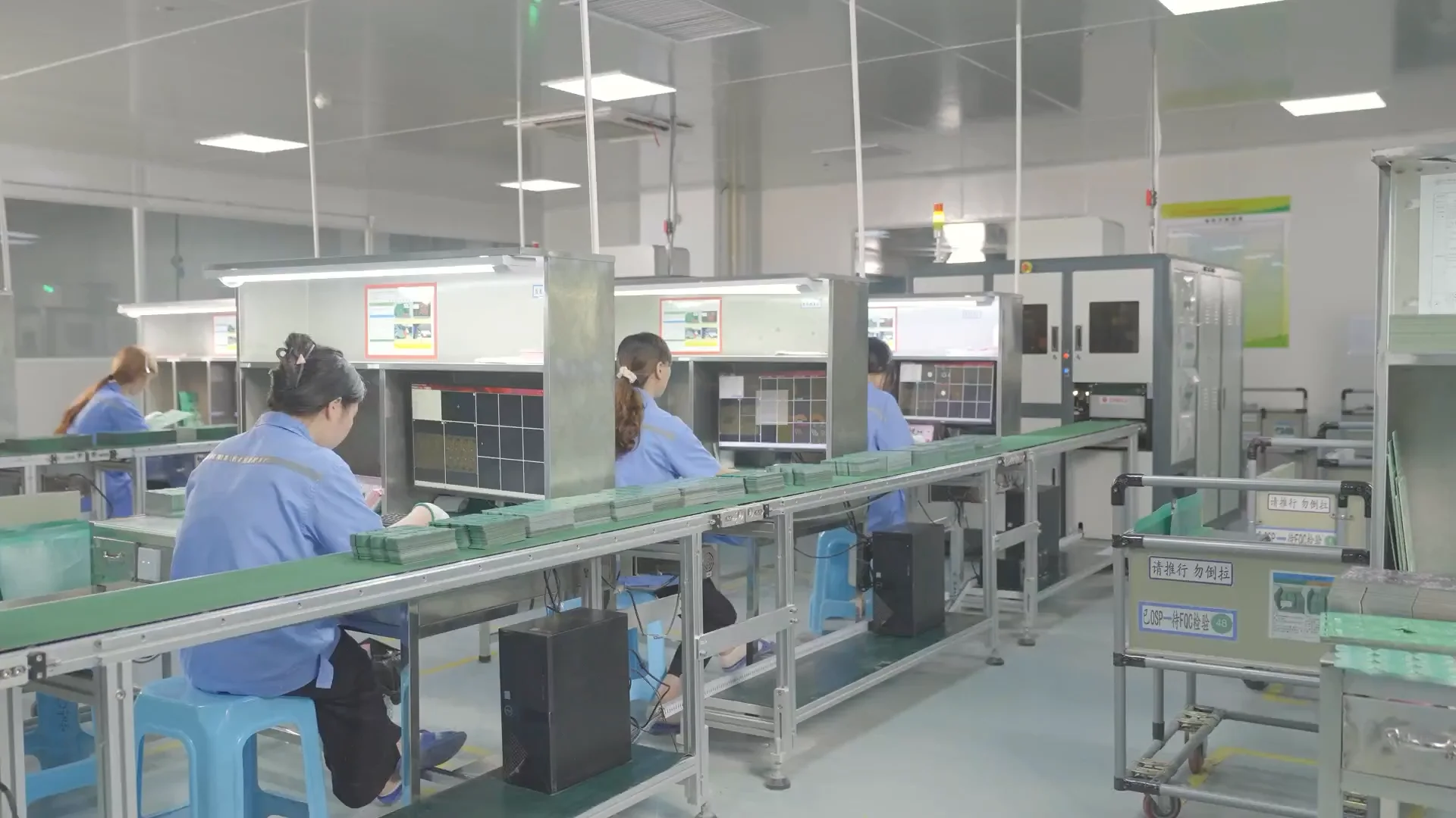
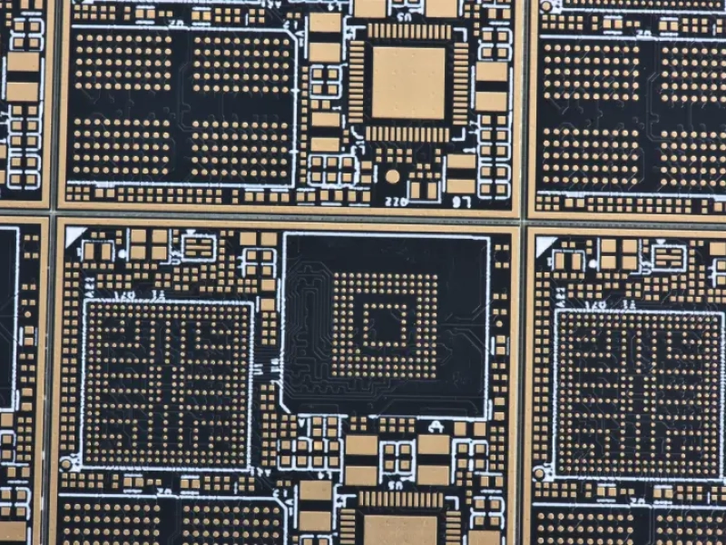
Finished-board visual inspection. This photo does not confirm trace current capacity or return-path performance.
After a single-sided layout is routed, count the nets that still need jumpers. Check whether the ground and power loops are complete, whether the outline grew to allow traces to detour, whether sensitive signals cross high-current paths, and whether copper has been split into disconnected areas. If several coupled detours or jumpers are needed to solve these issues, a double-sided layout may be easier to maintain.
Also review how revisions affect the rest of the design. A new test point, a replacement connector, or a changed power route can alter the planned jumpers and return paths. After each change, regenerate the netlist, rerun the design-rule check, and inspect the affected copper, pours, and drill data. Passing checks on an older revision does not prove the new revision is still connected correctly.
Do not compare only via count or copper-layer price. Put the schematic, outline, material, copper thickness, trace width and spacing, hole types, and surface finish in the same quote package. Refer to KnownPCB's single-sided PCB page for the existing product scope and its quality management page for manufacturing and inspection records. For prototype builds, submit the files to KnownPCB's high-mix, low-volume prototype service. If you need to discuss DFM assumptions, contact KnownPCB's engineering team.
No single trace width fits every board. Set the electrical requirement from current, copper thickness, allowed temperature rise, and route length, then check the fabricator's process capability. Controlled-impedance signals also depend on the stackup and dielectric properties.
Yes. Ground copper can share the same face, but a pour is not automatically a continuous reference plane. Check gaps, slots, isolated islands, and narrow connections, and confirm that the return network remains connected.
There is no universal count. Check whether jumpers cross sensitive signals, force power or return current to detour, enlarge the board, or make inspection harder. If several problems occur together, compare a double-sided layout.
 | Download our design guidesfor better PCB designing and manufacturing These are some of the design guides designers and engineersdownload the most:
|
Proven by 7 industries, 4000+ customer projects
Please contact us at sales@knownpcb.com, ask for engineering support here or use the form below to reach out to KnownPCB | Get In Touch Today |