Blog & Design Guide

RO4350B vs RO4003C is a material decision that can change a transmission line before the layout changes at all. The laminate name controls which dielectric data the engineer should use, while the ordered thickness, copper foil and finished construction determine how that model becomes a board. A substitute that looks close in a quotation still needs an electrical and manufacturing review.
Start with the requirement that cannot move. A flame rating, an insertion-loss budget or an approved material list may rule out one option before purchasing compares price. If both grades remain candidates, compare the same property under the same test conditions. Mixing a process dielectric constant for one laminate with a design dielectric constant for the other gives a misleading comparison.
Keep the copper option in the comparison record as well. If an alternative quote changes foil thickness or surface treatment, identify that change separately from the laminate grade so the engineer can assess its effect on the same circuit geometry.
Material decision points
Both grades belong to the RO4000 hydrocarbon ceramic laminate family. Rogers publishes different process and design dielectric constants because the measurement approaches serve different purposes. The following values come from the linked RO4000 data sheet, rather than from a board supplier's material table.
| Property and condition | RO4003C | RO4350B |
|---|---|---|
| Process Dk, clamped stripline, 10 GHz and 23°C | 3.38 ± 0.05 | 3.48 ± 0.05, subject to thickness note |
| Design Dk, differential phase length method, 8–40 GHz | 3.55 | 3.66 |
| Typical Df, 10 GHz and 23°C | 0.0027 | 0.0037 |
| UL 94 entry for standard grade | N/A in the cited data sheet | V-0 |
The Rogers RO4000 laminate data sheet notes a different process Dk for 4 mil RO4350B and qualifications on design Dk and LoPro constructions. Its typical values are not automatic specification limits. Check those notes against the exact ordered construction before transferring any number into a drawing.
A design tool also needs the geometry and frequency context for its material model. Save the source revision and the chosen Dk convention with the simulation. If an old stackup says only “Dk 3.48,” ask whether this is a purchasing requirement, a solver input or a measured value. Those labels prevent the same number from quietly acquiring a different meaning in the next revision.
A dielectric change affects the field around a conductor. Recalculate the critical lines using the proposed substrate, finished copper dimensions and reference-plane separation. Review electrical length as well as impedance. A filter, coupler or matching section can depend on phase even when its line impedance remains acceptable.
Keep the loss calculation separate from that impedance calculation. A lower laminate Df can help the dielectric part of the loss budget, but the finished path also includes conductor loss, copper surface profile, transitions and launches. A catalog Df comparison cannot establish the insertion loss of the complete board.
For a short matching network, component placement and pad geometry may deserve more attention than a long-line loss estimate. For an antenna feed network, accumulated phase and path consistency can dominate the review. Write down which response would make the material change fail, then choose the measurement or simulation that can evaluate it. Otherwise, an impressive data table can distract from the circuit's actual constraint.
The board photograph below provides context for patterned high-frequency copper features. A photograph cannot identify the laminate grade or verify the loss assumed in a simulation.
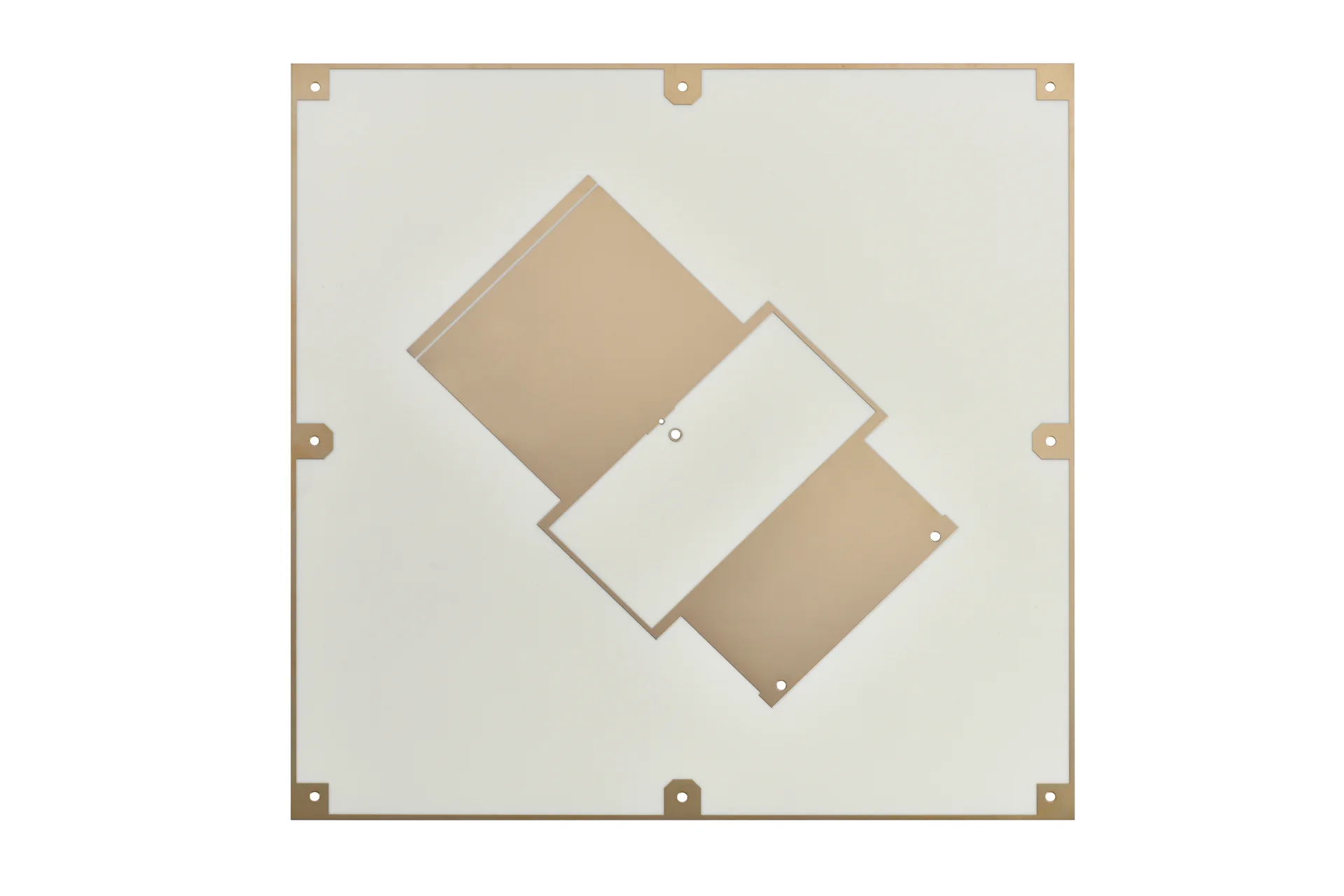
Patterned copper provides RF board context; material identity and electrical properties require separate records.
The purchase description should identify the grade, nominal dielectric thickness and copper option. For a multilayer board, identify the bonding materials and the location of every RF layer. The phrase “Rogers board” leaves too much open for a design whose response depends on a particular dielectric spacing.
KnownPCB's RF and high-speed PCB manufacturing page describes supported material families and hybrid constructions. Use it to start a review of the proposed build. Material availability, production geometry and inspection requirements still need to be resolved for the individual order.
Ask the fabricator to return a marked stackup before artwork release. It should distinguish starting foil from finished copper and show which values are nominal. Where the manufacturer proposes a width adjustment to meet impedance, approve the permitted change explicitly. A width change that is harmless on a uniform feed line may disturb an RF component footprint or a deliberately coupled structure.
Processing compatibility should be checked at the material-system level. The Rogers RO4000 processing guidelines discuss bonding, drilling and hole preparation for this family. A published starting point supports engineering review; it should not be pasted into an order as a universal press or drill recipe.
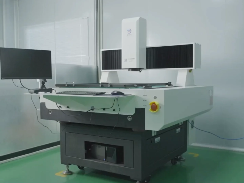
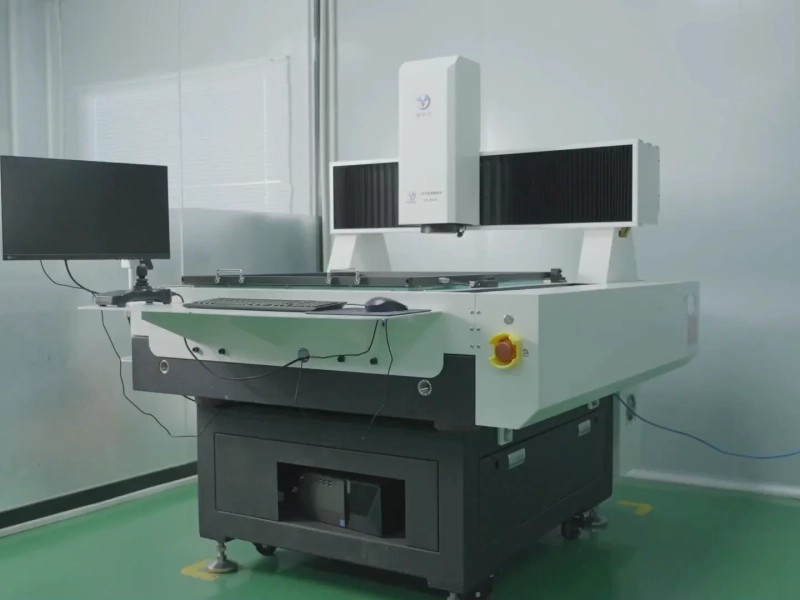
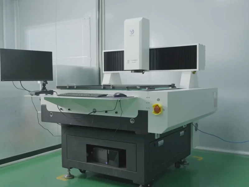
Lamination equipment belongs to that manufacturing context. The image below does not show the bond cycle, material assignment or a qualified construction for this article.
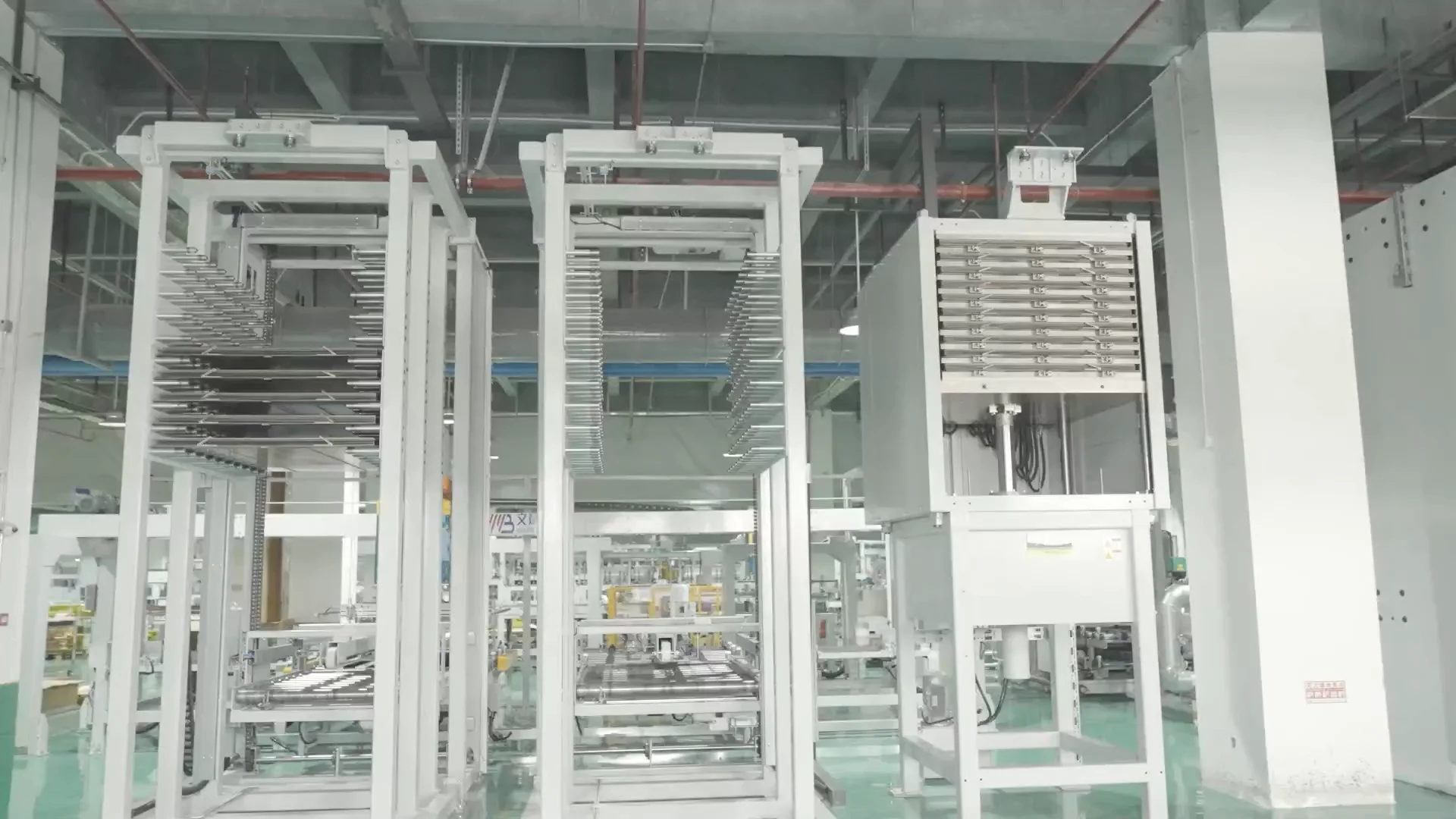
Lamination equipment is shown as process context, without implying a specific material or press cycle.
When purchasing receives an alternative laminate offer, keep the current approved build as the reference. Compare the proposed grade and copper configuration against it, then identify which design outputs need another check. Record the reason for the change, the approving engineer and the revision that will first use it.
Finish the review with a short decision record: unchanged requirements, changed model inputs, approved geometry changes and the evidence required from the trial lot. The result might be approval, rejection or approval limited to a particular product revision. That limit matters when several boards share a supplier but do not share the same RF margin.
The broader relationship between design targets, manufacturing control and measured results is covered in KnownPCB's controlled-impedance manufacturing article. For a material decision, bring that review back to the exact RF paths and laminate construction under consideration.
Retain the decision with the first production order using the alternative. Future buyers need to know whether approval covered the whole material family or only a particular thickness and copper combination. Otherwise, a limited trial can gradually become an unrestricted substitution rule without an engineering decision.
Send the proposed material, approved stackup and critical response requirements to request a laminate and stackup review. Include any restriction on substitutions so the quotation and engineering response address the same build.
Proven by 7 industries, 4000+ customer projects
Please contact us at sales@knownpcb.com, ask for engineering support here or use the form below to reach out to KnownPCB | Request a Manufacturing QuoteInclude your quantity, target delivery date and key requirements. File handling and NDA information. |