Blog & Design Guide

An FR4 Rogers hybrid PCB stackup needs a layer-by-layer reason for mixing materials. Place the specified RF dielectric where the electrical field and signal path require it, then decide how the remaining layers will carry control, power and other signals. A cost proposal becomes usable only after the whole stackup can be built and verified.
The release decision is often delayed because three different documents appear to describe the same board: a layout stackup, a quotation stackup and a factory build proposal. Compare them before choosing the material combination. Differences in a bond layer or reference plane can matter even when all three documents show the same total thickness.
Hybrid stackup release
Begin with the critical transmission lines. Identify their signal layer, reference plane and the dielectric region between them. A microstrip on an outer surface interacts with a different environment from an internal stripline. A coplanar structure also depends on its adjacent ground geometry. Merely assigning a Rogers core to the board does not describe any of these structures.
Next mark the routes that leave that region. An RF signal may change layer through a via, connect to a launch at the board edge or cross a region used by digital control. Review the reference path at each transition. Keeping a low-loss dielectric beneath a straight trace will not repair a poorly defined launch elsewhere in the channel.
Give the non-RF layers the same attention. A fast digital interface can have its own loss and timing requirements even if it is not part of the RF section. Decide whether its proposed FR4 system meets the product's requirements using the relevant material data and channel model. “Non-RF” does not mean that the dielectric choice is unrestricted.
Keep RF material grade, glass style where relevant and copper configuration visible in the stackup. Give bond layers names too. An adhesive or prepreg between two cores becomes part of the finished dielectric system and can affect the electrical field when it lies close to the controlled line.
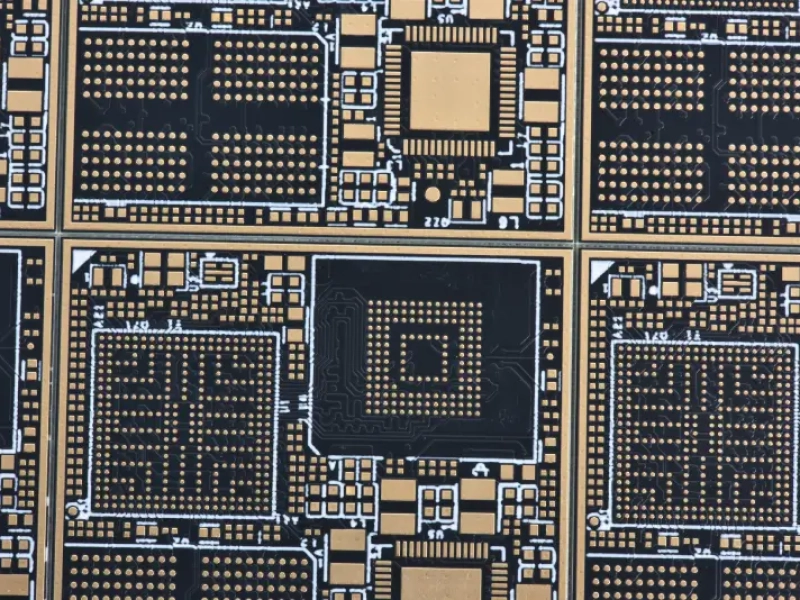
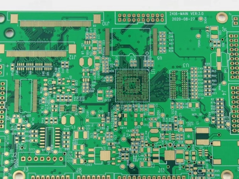
The product image below shows patterned copper and plated holes on an FR4/Rogers board from the local material library. It is an external board view, so it does not establish the internal layer sequence.
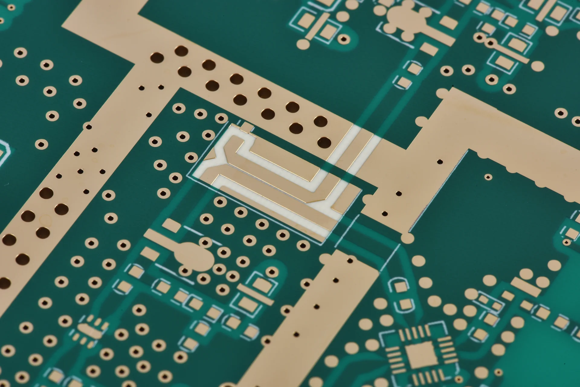
An external hybrid-board view illustrates the product; its internal materials and layer order are documented separately.
KnownPCB's FR4/Rogers hybrid manufacturing case describes a particular mixed-material project. Use that case for manufacturing context. The present decision is whether your proposed layer map, bond system and release documents define a workable construction.
Ask the fabricator which bonding system it proposes and why it suits the selected cores. Its cure requirements, flow and copper-fill needs must fit the construction. Use the material supplier's processing documentation as the starting point, then resolve the production proposal with the factory. A press recipe borrowed from a different hybrid is not a release specification.
Rogers' technical note on RO4000/FR4 hybrid flatness explains the selective use of RF materials and discusses construction-dependent warpage. That supports reviewing material balance and process compatibility together. It does not provide a single warp prediction for every mixed stackup.
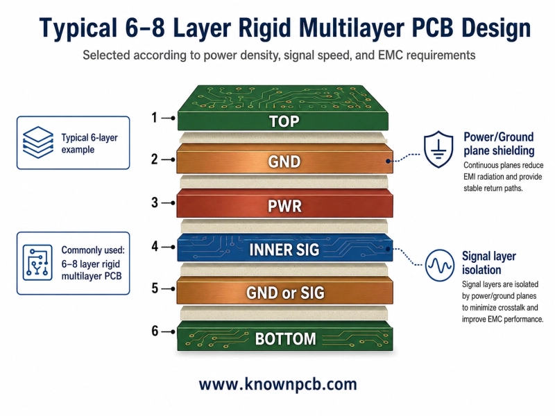
The mechanical review should include copper distribution, core placement and the finished board's handling requirements. Symmetry is useful, but a symmetric layer count alone does not prove a balanced construction. Different dielectric systems and copper patterns can remain on opposite sides of an apparently symmetric drawing.
A through hole encounters the materials along its full depth. The approved drilling and hole-preparation route therefore needs to address the combined structure. Identify the material families to the factory rather than relying on a generic desmear note. RO4000 hydrocarbon ceramic laminates and PTFE laminates should not be treated as interchangeable processing categories.
Hole acceptance also needs a defined inspection basis. Select the relevant hole structures and agreement on cross-sections or other required evidence before the trial build. The aim is to obtain a result that answers the construction question, rather than adding inspection after a failed board leaves everyone unsure what was sampled.
The lamination area below gives production context for bonding multilayer structures. Its appearance does not confirm the materials, temperatures or pressure used for a particular order.
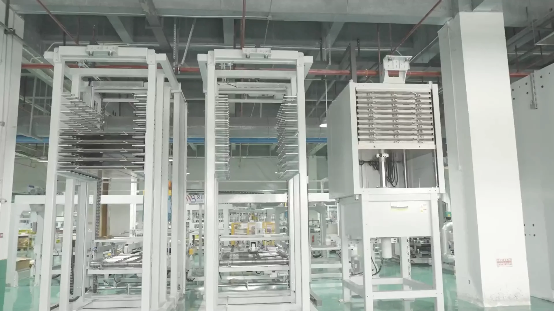
Lamination equipment provides process context; the approved build record defines the actual hybrid bonding route.
Separate stock-core thickness, pressed bond-layer thickness and finished board thickness. A total-thickness tolerance cannot stand in for a critical dielectric-spacing requirement. Ask which values the fabricator controls and how the trial lot will confirm them. When a change moves a signal closer to its reference plane, send the updated construction back to the electrical model.
For the material family's processing context, consult the RO4000 circuit processing guidelines. Keep those recommendations distinct from the factory-approved values for the complete hybrid.
A release record can be short if it names the unresolved decisions clearly. Put the designer's requirement and the manufacturer's proposal beside each other. Close each difference with an approved value, an allowed range or a documented trial requirement. Leave no row to be inferred from an email subject line.
| Decision | Release evidence |
|---|---|
| RF layers and their references | Approved layer map and impedance structures |
| Materials and bonding system | Named grades, copper options and permitted substitutions |
| Geometry changes | Updated model and written artwork approval |
| Trial-lot acceptance | Agreed samples, records and acceptance criteria |
Only then compare the mixed build with an all-RF alternative. Include engineering, available material sizes, coupon space and trial verification in the comparison. A lower material bill may still require extra engineering or a different production panel. Quote the same approved performance and evidence requirements for both alternatives.
The KnownPCB RF and high-speed manufacturing page is the service entry for this review. To resolve a proposed hybrid, send the layer map and material restrictions with the critical net requirements. Request one returned stackup revision that both engineering and purchasing can reference.
Proven by 7 industries, 4000+ customer projects
Please contact us at sales@knownpcb.com, ask for engineering support here or use the form below to reach out to KnownPCB | Request a Manufacturing QuoteInclude your quantity, target delivery date and key requirements. File handling and NDA information. |