
Blog & Design Guide

The adhesive vs adhesiveless flex PCB choice concerns the bond between copper and the base dielectric. It does not describe every bond in the finished circuit. An adhesiveless copper-clad core can still receive an adhesive-backed coverlay, a bonded stiffener, or bonding materials in a multilayer structure. Read the whole stack before deciding what the label means for your design.
An adhesive-based core has a separate adhesive layer joining the copper foil to the base film. An adhesiveless core omits that separate bonding layer at that interface. The finished board can use either core as part of a larger construction. The purchasing decision is therefore a comparison of specified material systems and their processing, rather than a competition between two universal performance grades.
| Item to compare | Adhesive-based core | Adhesiveless core |
|---|---|---|
| Copper-to-base-film bond | A separate adhesive layer forms the bond | No separate bonding adhesive at that interface |
| Stackup information | Include adhesive type and thickness | Identify the actual laminate product and construction |
| Other adhesive layers | Coverlay and local bonding may also be present | Coverlay and local bonding may still be present |
| Approval basis | Review the complete finished stack for the application | Review the complete finished stack for the application |
On this page
Removing a core adhesive layer can reduce thickness at that interface, but it does not tell you the total finished thickness. Compare the same copper thickness, base dielectric thickness, protective layers, and bonding arrangement. If two quotes use different values elsewhere, attributing the whole difference to the word adhesiveless can lead to a misleading material comparison.
Thickness must also be assigned to regions. A connector area with a stiffener has a different mechanical role from a free tail. Specify the connector thickness at the location where it is measured, and show where the support ends. Do not add copper or a stiffener across the active span simply to meet a contact thickness requirement that applies only at the connector.
Altium's discussion of flex stackups and protective layers notes that an adhesiveless laminate removes the core bonding adhesive while coverlay and multilayer bonding materials may remain. That distinction helps explain why a datasheet for one core is insufficient to describe a completed flex assembly. Request a stackup listing every material layer used in the relevant region.
The tail and contact areas in the photograph can be checked against the outline drawing. Their internal construction cannot be identified by the amber color or the surface appearance. Use the material callout and supplier records to distinguish core systems; product photographs are useful for shape and layout, not for confirming a hidden adhesive layer.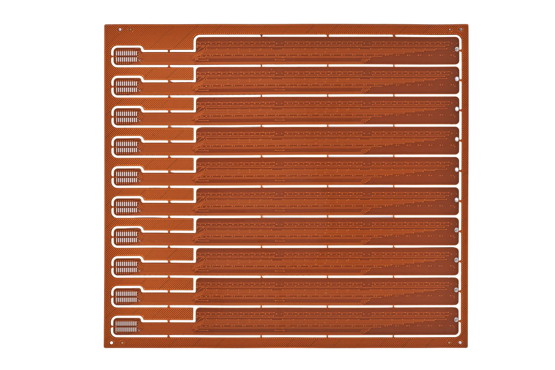
The tail outline and contact areas are visible; internal adhesive layers cannot be identified from this photograph.
Electrical calculations need the same level of detail. A trace sees its surrounding dielectric and reference conductors, including relevant adhesive and coverlay. Reusing a trace width from another core system without reviewing that geometry can change the transmission-line environment. Keep the approved stackup tied to the impedance requirement rather than assuming two polyimide products behave identically.
For a moving circuit, examine the complete active span: finished thickness, copper type, conductor layout, protective layers, and supports. A thinner construction can help meet packaging and deformation requirements, but the laminate name alone does not establish fatigue life. A qualification claim should identify the construction and motion conditions under which the sample was tested.
For a circuit formed only during installation, check the forming path and any later service handling. The same assembly may include flat supported areas, a curved free span, and a connector tail. One material description covers the laminate, while several mechanical conditions govern how that laminate is used. Keep those conditions visible when the supplier proposes a different core.
Review the material manufacturer's properties and the fabricator's qualified process against the intended assembly exposure. Include relevant adhesive layers instead of assessing the base polyimide alone. Reflow, bonding, and any subsequent repair operations can expose a finished construction to heat more than once. The acceptance basis should identify the finished product requirements and the evidence used to support them.
Avoid translating a material family into a blanket service-temperature promise. A property measured on a laminate specimen is not automatically the allowable temperature for a connector bond, an assembled circuit, or a repeatedly moving tail. Identify the property, test method, and component of the stack to which the value applies before using it in a design decision.
Ask the fabricator to quote the exact proposed laminate and explain whether it is routinely stocked. Core price is only one input. Yield, panel utilization, processing, inspection, and qualification can affect the finished price and lead time. A cheaper material that forces a redesign or a new approval may cost more over the first production order than the initial quote suggests.
KnownPCB's confirmed product scope includes polyimide systems, adhesive and adhesiveless constructions, coverlay, and stiffeners. Start at the FPC manufacturing page for the relevant product scope. The project review still needs the exact laminate, region stackup, motion duty, and assembly conditions; the availability of a material family does not qualify every possible construction.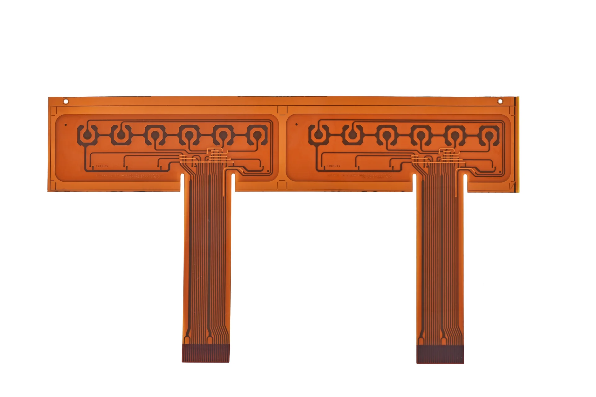
Wide circuit areas and narrow tails can have different support and bending requirements.
The public IPC-4204B scope and contents identify flexible metal-clad dielectrics and distinguish base material, adhesive, and metal-cladding designations. Its scope also explains how extra thickness details can be given on drawings. This is a useful reason to specify the construction clearly rather than write only PI or adhesiveless in a general note.
Identify the approved laminate product or agreed material designation, copper construction, individual thicknesses, and acceptable tolerances. Name the coverlay and bonding materials separately. If the fabricator is allowed to propose alternatives, require a written comparison against the properties and processing conditions that matter to the application. Equivalent should have an agreed meaning before the purchasing team accepts it.
Record substitutions as changes to the manufacturing package. The review should address thickness, connector fit, bending, thermal exposure, and electrical requirements affected by the proposal. An alternative can be acceptable, but the approval should refer to a revision or change record so that the next order does not depend on remembering an email conversation.
If rigid sections are integrated into the board, review the rigid-flex construction scope as well. A rigid-flex stack adds region boundaries and bonding decisions that a core comparison alone cannot resolve. The flex core, rigid materials, and protective layers must be described together without confusing total board thickness with the thickness of the free flexible span.
To compare two candidate materials, send the proposed flex stackups for engineering review with the installed geometry and assembly requirements. Ask the response to identify every changed layer. That provides a usable basis for selection and preserves the material decision when the order returns for production.
July/23/2026PCB Common DFM Mistakes and Solutions
October/10/2026SMPS PCB Layout: Hot Loops, Return Paths, and EMI Checks
March/10/2026What are the design challenges of a 4+10+4 HDI PCB?

February/26/2026HASL vs ENIG vs Hard Gold: Cost, Solderability, Flatness and Wear Resistance
October/09/2026Single-Sided PCB Routing: Jumpers, Return Paths, and Width
Proven by 7 industries, 4000+ customer projects
Please contact us at sales@knownpcb.com, ask for engineering support here or use the form below to reach out to KnownPCB | Request a Manufacturing QuoteInclude your quantity, target delivery date and key requirements. File handling and NDA information. |