Blog & Design Guide

Fine-pitch HDI boards can have correct copper pads and still lose solderable area when mask openings shift or narrow bridges merge. A similar white mark may come from silkscreen, not mask. Start by locating the faulty layer.
Follow the defect from Gerber preview to source edit and release. Compare copper, solder mask, paste, and silkscreen separately. The correct opening depends on the pad definition and the fabricator’s rules.
In this article
Start with the top or bottom solder-mask Gerber that shows the affected area. A mask file represents where the board will remain uncovered, but CAD tools and CAM viewers can display positive or negative images. Confirm the layer name and polarity before deciding that an opening is missing. Then compare the same location on copper, paste, and silkscreen files.
| What the plot shows | Layer to inspect first | Possible source-file action |
|---|---|---|
| Mask covers part of a component pad | Solder mask and copper pad | Check pad shape, mask expansion, and local override before changing the footprint. |
| A thin strip between two openings disappears | Solder mask | Compare the remaining web with the agreed minimum, or discuss a shared opening. |
| A white mark crosses an exposed pad | Silkscreen | Move, trim, or remove the text or graphic in the silkscreen source. |
| A via looks open in the mask view | Via treatment note and mask layer | Confirm whether that via is open, tented, plugged, or filled and capped. |
Do not enlarge every opening because one pad appears covered. A global change can expose nearby copper or remove a needed mask bridge. Use a local edit unless the same error appears across a repeated footprint or layer.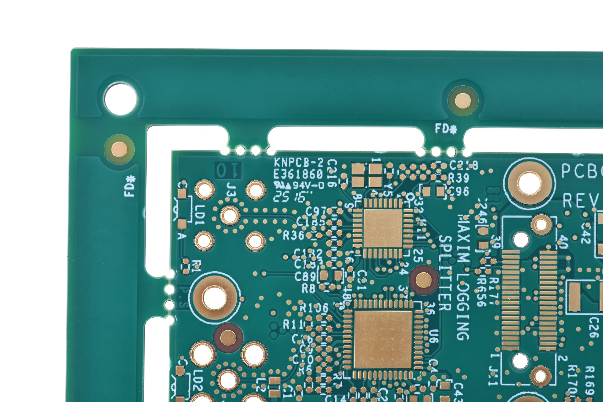
A 10-layer HDI board surface shows the mask openings and copper pads that should be checked as separate layers.
Four layers meet around a surface-mount pad. Copper defines the electrical land. Solder mask defines which parts remain exposed. Solder paste defines where assembly paste may be deposited. Silkscreen carries reference designators, polarity marks, and other surface text.
Open the copper and solder-mask files together and align their origins. Verify that the exposed shape belongs to the intended pad, not a nearby via or copper pour. Look for a global origin shift, a mirrored bottom layer, a wrong layer assignment, or a unit conversion before editing a footprint. If the source CAD view and the plotted files disagree, correct the export or layer mapping before making geometry changes.
A solder-paste aperture is not a solder-mask opening. Reducing a paste aperture can change the amount of paste used in assembly, but it does not uncover copper that is covered by solder mask. If the pad is exposed correctly on the mask plot but the paste plot is smaller, route that question to the assembly drawing or stencil definition rather than changing the mask file.
The official KiCad PCB Editor documentation treats mask expansion, minimum web width, and mask-to-copper clearance as separate settings. It also notes that closely spaced openings may merge in the plotted output. Use this as a layer-checking reference, then set the actual values from the selected fabricator’s written rules.
Before changing a fine-pitch footprint, identify whether its pads are solder-mask defined or non-solder-mask defined. In a solder-mask-defined pad, the mask opening is smaller than the copper land, so the mask overlaps the pad edge. In a non-solder-mask-defined pad, the opening is larger and the copper edge sets the land. Either style can be appropriate for a given package. The footprint, assembly process, pad pitch, and fabricator’s registration limits decide which one to use.
A mask dam is the strip of solder mask between adjacent openings. If it is too narrow for the imaging and development process, it can break or merge with a neighbor. The minimum depends on the fabricator and board construction. Do not treat software defaults or another shop’s values as production rules.
KnownPCB's HDI table lists separate minimum dimensions for its 1-step, 2-step, and 3-step builds: a solder-mask bridge of at least 0.075 mm and a mask opening of at least 0.076 mm. These are two parameters, not the endpoints of one range. The any-layer/ELIC columns use stage-dependent or per-design conditions, which need confirmation for the actual construction. Confirm how it applies to the selected layer, mask, board construction, and acceptance plan during the DFM review. See the KnownPCB HDI PCB capability page for the broader HDI scope. The photo below shows a solder-mask development line as process context, not a measurement of this opening.
A solder-mask development line is shown as process context, not as evidence of a specific HDI opening measurement.
Separate openings preserve a mask bridge between pads when the fabrication rules allow one. A shared opening removes that strip and exposes a wider area. Shared openings can resolve an unmanufacturable sliver, but they also change the solderable surface and can allow solder to bridge during assembly. Do not replace every narrow dam with one large window without checking the package land pattern and the assembly requirements.
If a dam cannot be maintained, test the footprint against an approved mask-defined or shared-window option. Change only the affected footprint or pad override, and record the reason. A global expansion setting is easy to apply but can alter many unrelated openings at once.
Silkscreen overlap is a separate drawing problem. Reference text, polarity marks, and outlines should not cover an exposed pad or hide a polarity cue. Check the top and bottom silkscreen files after changing the solder mask because a mask edit can reveal copper beneath text that looked harmless in the CAD composite. Move or trim the text in its own source layer, then replot it.
Via treatment also needs an explicit note. A mask opening does not say whether a via should remain open, receive a mask tent, be resin plugged, or be filled and capped. If the via is intentionally exposed, show its location and purpose. If it is part of an in-pad or stacked-microvia construction, use the project’s separate via definition and fill notes. Keep the mask layer from silently defining a process that belongs in the fabrication drawing.
Make the change in the CAD source when possible, then regenerate the manufacturing output. Editing a single Gerber by hand can leave the source design and released files out of sync. It also makes a later revision harder to audit. If a CAM adjustment is required, ask the fabricator to document the change and return the revised layer for engineering approval.
A focused edit usually follows this order:
Then run the design-rule check against the confirmed constraints. Review the Gerber plots at the affected BGA or fine-pitch connector, not only in a full-board thumbnail. Check both sides, repeated footprints, board edge, plated holes, and any shared openings. A design-rule pass is useful only when the rules match the fabricator’s current process and the file export includes the correct layers.
Include the corrected copper, solder-mask, solder-paste, and silkscreen files with the same revision and unit system. Add the layer map, stackup, package footprint or drawing reference, and any note that defines solder-mask style or via treatment. This lets the CAM reviewer identify which openings are deliberate and which are open questions.
Ask the fabricator to confirm any opening or bridge that is below its stated rule, and to identify whether it recommends a local mask change or a shared opening. The response should identify the affected reference designator or coordinates. If the review changes the footprint or mask geometry, approve the revised plot before releasing the files for fabrication.
For construction background, see the HDI board introduction. For a project review, send the layer-mapped files through KnownPCB’s contact page. A layer comparison preserves the intended pad and opening relationship in the next revision.

October/13/2026Prototype to Low-Volume PCB: Bare-Board Release Gates

May/13/20268 Layer PCB Manufacturing and DFM Guide

October/10/2026SMPS PCB Layout: Hot Loops, Return Paths, and EMI Checks

October/13/2026PCB RFQ Checklist for Comparable Bare-Board Quotes

October/09/2026ENIG Nickel and Gold Thickness: Drawings, XRF, and Reports
Proven by 7 industries, 4000+ customer projects
Please contact us at sales@knownpcb.com, ask for engineering support here or use the form below to reach out to KnownPCB | Request a Manufacturing QuoteInclude your quantity, target delivery date and key requirements. File handling and NDA information. |