
Large vs. Small PCB Manufacturers: Which Fits Your Project?
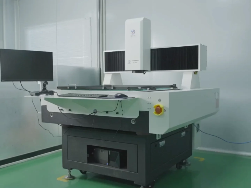
When choosing an HDI PCB manufacturer in China, you will generally come across two types of suppliers. One is large manufacturers, such as Victory Giant Technology, Kinwong, and Suntak. The other is small to medium-sized manufacturers, such as NextPCB and KnownPCB.
A steady project with stable production demand and an R&D project requires frequent revisions need different types of suppliers, the goal isn't finding the "best" factory overall—it's choosing the right PCB manufacturer based on your specific order volume and tech requirements.
Here is a quick look at how big and small-to-mid-sized suppliers compare:
Large PCB Factories: A Good Fit for High-Volume Production
- Capacity: Multiple production lines, support high-volume HDI PCB orders to support a stable supply chain.
- Cost: Huge output and bulk material purchasing can reduce the cost per board.
- Limitations: Their internal processes are slow when handling prototype HDI PCB orders, low volumes, or quick design tweaks. Since their lines prefer massive runs, their pricing for small orders isn't very competitive, and your project will have low priority.
Small-to-Mid PCB Manufacturers: A Practical Option for Prototypes and Low-to-Medium Volumes
- Capacity: They are highly flexible, making them the best fit for quick-turn prototypes, EVT/DVT engineering samples, and low-volume HDI board runs.
- Cost: Lower overhead and setup costs mean they offer highly competitive pricing for low-volume and prototype orders.
- Service: Direct engineering contact and flexible scheduling make it better for design changes or urgent orders.
- Limitations: They invest less in high-end automation and testing equipment. For massive production runs (tens of thousands of boards), their long-term yield consistency may fall short compared to tier-1 manufacturers.
If you are currently in the R&D prototyping or small-to-medium volume phase, KnownPCB specializes in these exact needs by providing No MOQ HDI PCB manufacturing and one-stop PCBA services. Explore KnownPCB's HDI services to see if they fit your project.
5 Key Capabilities to Check When Choosing an HDI PCB Manufacturer
Matching your order size to the right factory tier is only the first step. Because high-density interconnect (HDI) technology involves fine traces, small vias, and tight process control. Whether you need stable volume production or flexible prototype support, evaluate your candidate HDI PCB supplier on these 5 technical capabilities before signing a contract:
1. HDI Capabilities: Are Your Designs Within Their Mature Yield Range?
Don't just ask, "Can you make an 8-layer board?" and don't blindly trust a website that claims they can do 1+N+1, 2+N+2, 3+N+3. Being able to build an HDI PCB doesn't mean they can manufacture your specific project reliably.
You need to know the difference between their standard capability and their process limits. It's better to check if they have produced boards with similar stack-ups, via structures, and board thicknesses. For example, KnownPCB's minimum laser via size for 1-to-3-stage HDI is about 0.076mm, and the minimum trace width/spacing for 2-stage HDI is 3/3 mil. However, these figures still need to be checked against dielectric thickness, copper weight, and pad size. Meeting one minimum specification does not mean the complete design is manufacturable.
2. Production Equipment: Check the Complete Process
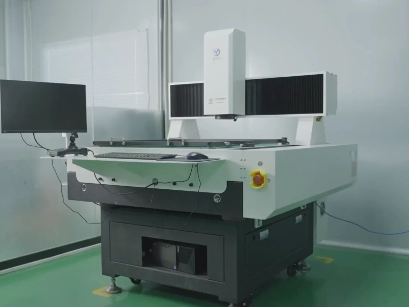
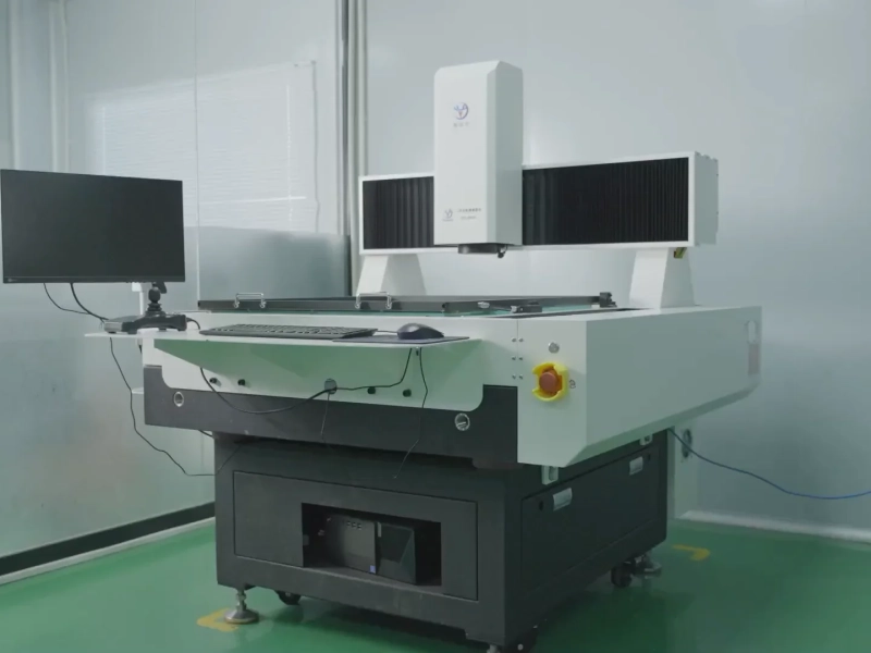
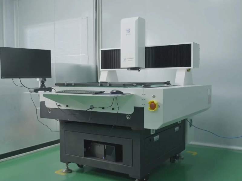
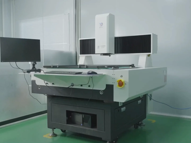
HDI PCB fabrication involves laser drilling, laser direct imaging (LDI), multiple lamination cycles, copper via filling, and automated optical inspection (AOI) . Having a single laser drill machine doesn't mean a factory has a complete setup.
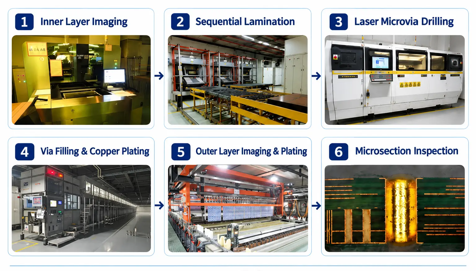
Take 3/3 mil traces and spaces as an example, the factory also needs matching etching control and optical inspection. If your design uses stacked microvias, you should also ask how they handle via filling, surface flatness, and layer-to-layer registration. Tier-1 factories usually have more extensive automation and equipment investment. If you choose a smaller manufacturer, pay attention to which processes are available in-house. And if you are going to do a factory audit, you can ask them to walk you through the actual workflow of a real similar board.
3. Quality Certifications & Testing: Match Them to Your Application
Check certifications that are relevant to your product:
- Consumer Electronics, communication modules and general industrial controls: ISO 9001 is a baseline for reviewing the manufacturer's quality management system.
- Automotive Electronics (BMS, Main Controllers): Check IATF 16949 certification, and verify if they have relevant automotive production experience.
- Medical Devices (Monitors, Diagnostic equipment): Look for ISO 13485 certification, and check their ability to handle strict production records, change control, and batch traceability.
For quality testing, specify how the factory uses AOI, electrical testing, X-ray, and micro-section analysis to catch flaws. For instance, a 100Ω differential impedance requirement with a ±10% tolerance means an acceptable range of 90–110Ω. If your project demands a tighter ±5% (95–105Ω), confirm with them on manufacturing and testing conditions before ordering. For microvias and hole-wall copper, confirm the inspection method, sampling plan, and acceptance criteria, don't assume a board is reliable just because it passes a basic continuity test.
4. Engineering Support: Can They Spot Manufacturing Risks Before Production?
A useful design for manufacturing (DFM) review should cover the stackup, impedance, via structures and other features that may affect fabrication before your board hits the line.
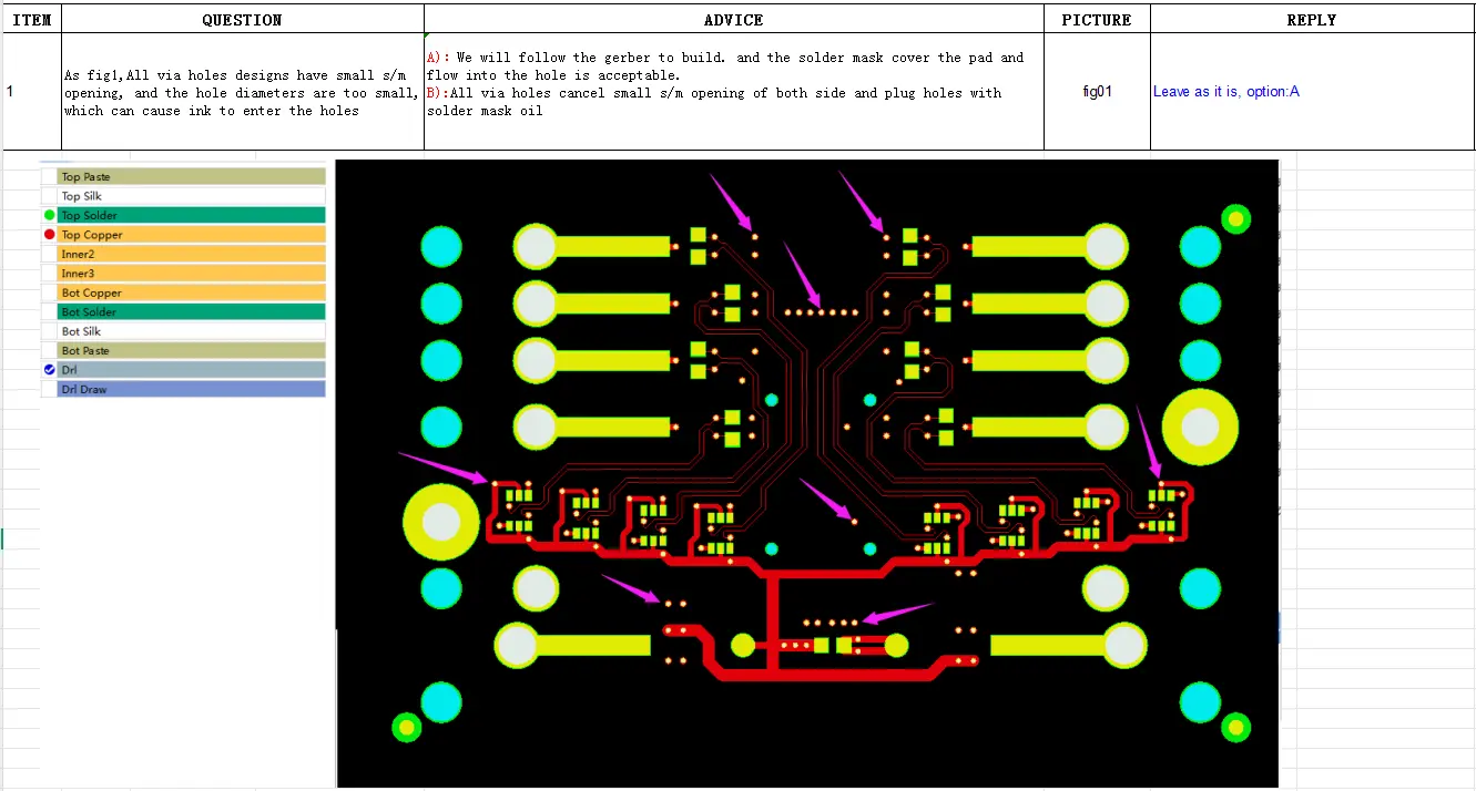
For example, if the solder mask openings around vias are too small or missing, the engineer should confirm whether the vias should be tented, plugged, or left exposed, and suggest changes where needed. Any changes to stack-ups, trace widths, or via structures should be documented and approved before manufacturing starts. This is especially helpful for HDI PCB manufacturing because small changes can affect several parts of the design.
5. Lead Time and Cost: Compare Quotes on the Same Basis
When choosing HDI PCB suppliers, send the same Gerber files and fabrication requirements to all candidates. Don't just compare the final number, see who asks the most specific technical questions, who provides the most transparent line items, and who clearly defines their responsibilities.
Make sure you know exactly when the lead time starts—does it include the engineering query (EQ) window, sourcing specialized materials, and final inspection? For both standard and quick-turn HDI PCB fabrication, check minimum order quantities (MOQ), their standard and expedited lead times, recent On-Time Delivery (OTD) rates for similar orders, and whether the quote includes electrical tests, impedance reports or other special testing fees. A clear quote helps you to compare HDI PCB manufacturing costs and avoid unexpected charges after ordering.
Frequently Asked Questions (FAQ)
1. What is the difference between an HDI PCB and a standard multilayer PCB?
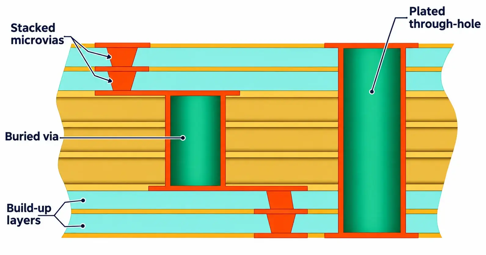
An HDI printed circuit board uses microvias (blind, buried, or stacked) and ultra-fine traces to achieve higher routing density. The main differences are the interconnect structure and feature sizes, not just the total layer count.
2. Which Products Need HDI PCBs?
Common applications include smartphones, wearables, 5G and communication modules, and high-density computing boards. If your design is extremely space-constrained and uses fine-pitch BGAs (Pitch ≤ 0.5mm) where standard multilayer boards cannot route the signals out, you need an HDI board.
3. Why Do HDI PCBs Cost More Than Standard PCBs?
Laser drilling, microvia filling, fine-line etching, and sequential lamination add process steps and require tighter control. They can also increase material loss during manufacturing. The exact price depends on your via structure (1-stage, 2-stage, 3-stage), chosen laminate materials, and your total order volume.
4. Can I order low-volume custom HDI PCBs and prototypes?
Yes. Suppliers like KnownPCB support custom prototyping and low-volume production with No MOQ. HDI process and final price must be confirmed after reviewing your design files.
5. What Is the Typical Lead Time for HDI PCB Manufacturing?
KnownPCB lists the following reference production times: 7–10 days for 1-stage HDI, 8–15 days for 2-stage HDI, and 12–18 days for 3-stage HDI. The actual lead time will depend on design complexity, material stock, and current factory line capacity.