Blog & Design Guide

Do not copy a creepage or clearance value from a generic table for a high-voltage power-supply PCB. The required distances depend on the equipment, working voltage, transient overvoltage, pollution degree, material group, altitude, and applicable product standard. Define the isolation boundary first, then calculate and check it under the specified standard.
This article focuses on bare-board DFM files. It explains how the two distances are measured, how to mark an isolation boundary in the design data, and which material and drawing details a fabricator needs. A board fabricator can check whether the data is clear and the structure is manufacturable. Gerber files or an FR-4 label alone cannot establish safety compliance for the finished equipment.
A power board may contain low-voltage control, switching nodes, and a high-voltage input area. The voltage stress and insulation purpose differ between pairs of nets. Designers need to identify which conductors require safety isolation and which only need functional insulation. Without that distinction, a DFM reviewer cannot know which shortest paths to check.
Table of contents
Clearance is the shortest distance through air between two conductors. Creepage is the shortest path along the surface of an insulating material. They address different insulation failure conditions and use different measurement paths. TI's power-supply design seminar links transient overvoltage to clearance and lists working voltage, material group, and pollution conditions among the inputs to creepage calculations.
The copper-to-copper spacing shown on a board is not always the required safety distance. The starting point may be a pad, copper pour, exposed via wall, or conductor near the board edge. The endpoint may be on another layer, a metal part, or an accessible connector. For each boundary, identify the conductors and trace the relevant path through air and along the insulating surface.
If the design uses a slot to lengthen the surface path, also check the shortest air distance between the conductors, their positions relative to the slot edges, the board thickness, and the routing tolerance. A slot does not automatically meet every creepage or clearance requirement.
First confirm the target market, equipment category, and whether the insulation provides functional protection or protects people from hazardous voltage. Then establish the working voltage, voltage under normal and abnormal conditions, transient overvoltage, and overvoltage category. The required insulation type, such as basic, supplementary, double, or reinforced insulation, must also come from the product safety design and applicable rules.
IEC 60664-1 provides a general insulation-coordination framework for low-voltage equipment. The IEC Webstore lists a consolidated edition, IEC 60664-1:2020+AMD1:2025. This general standard does not replace the product standard. For example, IEC 62368-1:2023 covers audio/video, information, and communication technology equipment. Medical, motor-drive, photovoltaic, and other equipment must use the standard and edition that apply to their product scope.
The published scope of the consolidated edition covers equipment connected to low-voltage supply systems with rated voltage up to 1,000 V AC or 1,500 V DC, at frequencies up to 30 kHz, and includes guidance for higher altitudes. Review the actual voltage waveform and stress across the insulation. A converter's switching frequency alone does not determine which clauses apply to the entire insulation system. For equipment outside this scope, use a product standard that covers the relevant stress and insulation requirements.
Also establish the intended altitude, pollution degree, and insulation material group before calculating. Pollution degree describes the expected nonconductive contamination, condensation, or conductive pollution in the environment. Material groups relate to the insulating material's resistance to tracking. CTI data should come from the specified laminate supplier or an accepted test record. Do not infer a material group from the generic name FR-4.
Put these inputs and the standard edition in the project documents instead of marking only "high-voltage spacing" on the drawing. TI's method for high-voltage creepage and clearance includes working voltage, transients, overvoltage category, pollution degree, altitude, and material group. Confirm the current IEC edition in the IEC 60664-1 publication record. The IEC 62368-1 product-standard scope applies only to equipment covered by that standard. Use the applicable product standard and insulation grade to determine the actual values; do not substitute a web table.
Map the isolation boundary between the schematic and the PCB layout. Common examples include the power input and safety-low-voltage side, primary and secondary circuits, buses at different potentials, and accessible connectors or mounting hardware. The system architecture and product standard determine the boundary. Do not assume every supply has one straight primary-to-secondary barrier.
Mark the nets on both sides, copper keep-outs, and paths that need review in the PCB files. Check every copper layer, pad, via, slot, mounting hole, and board edge. The shortest route may pass around a pad or follow the board edge. Copper on an adjacent layer or a plated hole wall can also affect the path. Checking only the gap between two top-layer traces can miss the actual shortest distance.
Use consistent boundary identifiers on the stackup and mechanical drawing, then mark the corresponding copper layers and features on the Gerber or ODB++ review plots. This gives both engineering teams a shared coordinate and boundary name when discussing a location. A note such as "leave enough distance between primary and secondary" is not enough to create a repeatable inspection record.
If a boundary crosses the board surface, internal layers, and board edge, the report should state which requirement applies to each segment. Layer-to-layer insulation depends on the laminate, dielectric thickness, construction, and voltage stress. It is not a creepage path measured along the board surface. The fabricator needs to know which layers, holes, or mechanical features must stay fixed to identify a specific DFM conflict.
Include test points, connectors, screws, and metal supports near the isolation area in the boundary drawing. Separate reviews of the mechanical assembly and PCB layers can miss the shortest air path created after installation. Update the boundary drawing and spacing notes if the mechanical structure changes.
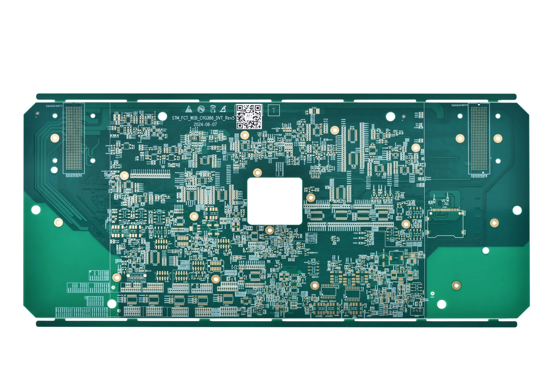
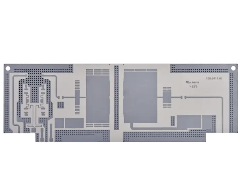
Multilayer heavy-copper PCB. The photo does not show a high-voltage clearance or insulation test result.
FR-4 is a common material family name, but it does not specify the CTI, material group, or safety rating of a particular laminate. Name the manufacturer, material series, and supporting test data. If the supplier substitutes the laminate, changes the glass-cloth construction, or changes the pressed thickness, recheck the design under the applicable standard.
Do not count solder mask as safety insulation by default. Whether a coating may change creepage or clearance requirements depends on the product standard, material evaluation, coverage, process control, and required validation. Without that evidence, the DFM review should assess conductor and base-material geometry; a green solder-mask bridge is not confirmed safety insulation.
Multilayer boards need both surface-path and layer-to-layer checks. Review the material and dielectric thickness in the stackup, and confirm that overlapping high-voltage nets, adjacent copper, vias, and board-edge structures meet the defined requirements. After adding a slot or cutout, check its width, length, location, and routing tolerance so that cutter deviation does not move a conductor into the safety boundary.
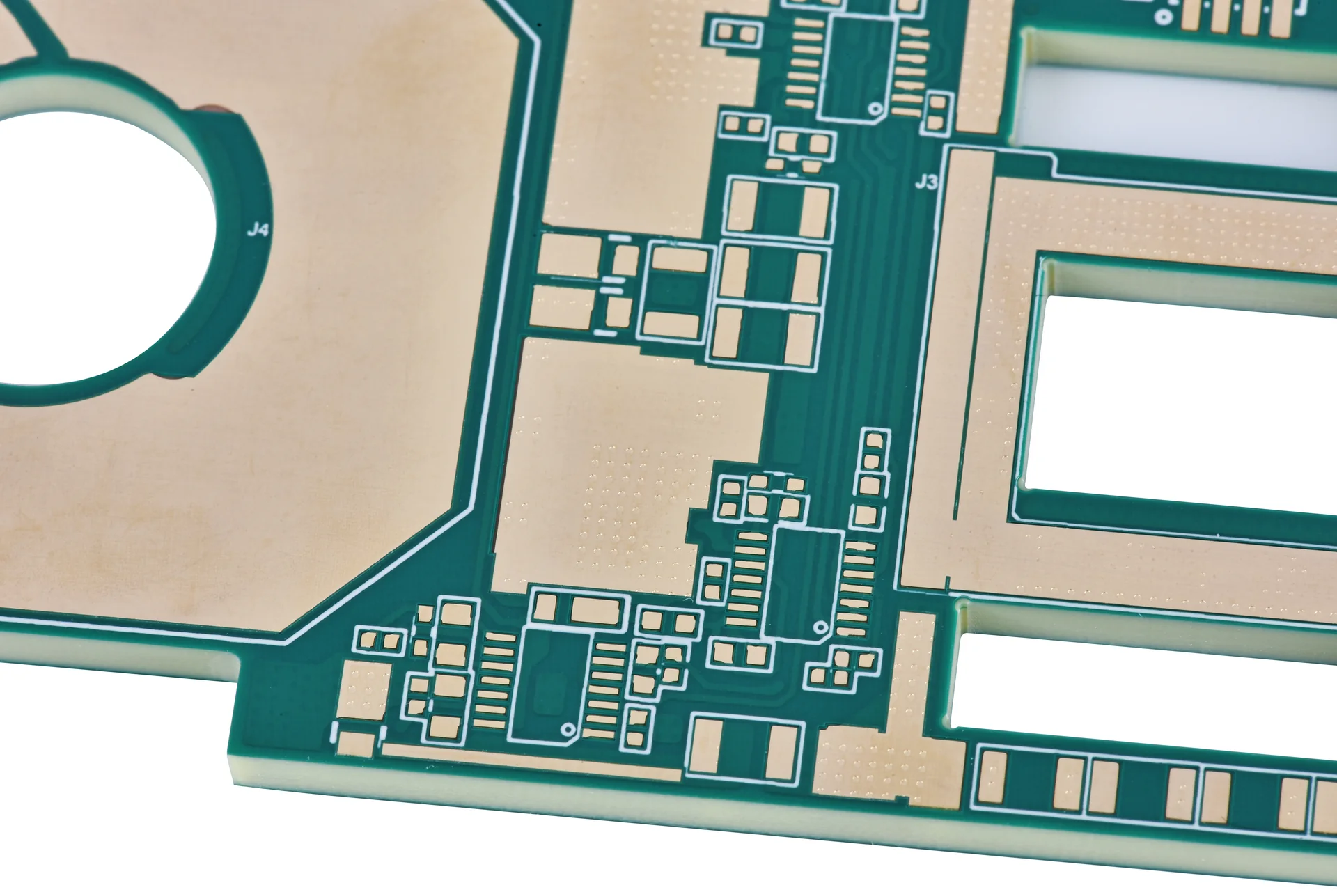
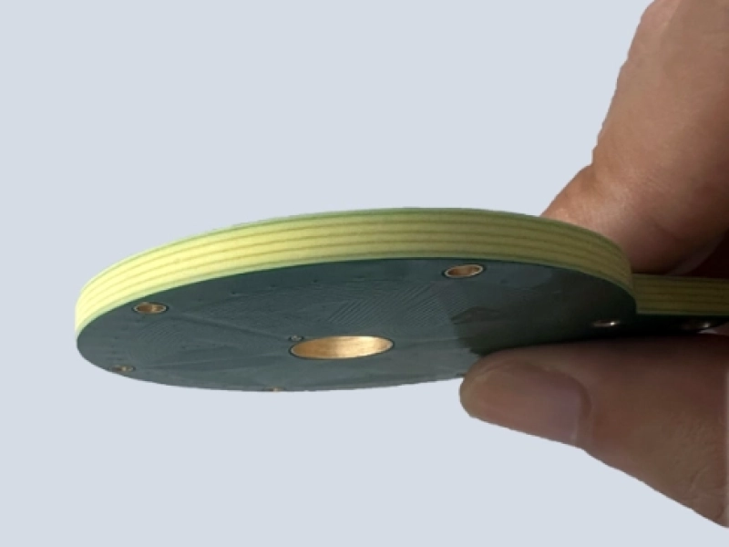
Via-in-pad heavy-copper PCB. This photo does not show a high-voltage isolation structure or test result.
A slot can change the path along the board surface without changing the shortest path through air. Its edges, width, and routing tolerance all affect the result. Recheck the complete geometry under the target standard before using a slot to address a spacing issue. Adding a slot is not a universal fix.
Useful review files include complete Gerber or ODB++ data, drill and slot files, stackup, finished board thickness, copper weight, laminate designation, and mechanical drawings. Add a high-voltage net or isolation-boundary drawing. Identify the nets on each side of the boundary, insulation target, standard edition, and conditions used for the review. Note special solder-mask openings and board-edge structures in the mechanical and fabrication notes.
A reviewable DFM checklist keeps the standard edition, input conditions, boundary location, shortest path, material evidence, and open questions in one record. The report should identify the affected layer, pad, or hole and state the geometry path and tolerance used. If a required material value or product standard is missing, mark it for confirmation instead of filling it with a default.
If dielectric-strength or withstand testing is required, define the nets, test voltage and duration, environment, sample count, and acceptance criteria first. A bare-board test can answer a board-level insulation question. It is not equipment certification and does not cover every isolation path through components, connectors, the enclosure, and the assembled product. The customer and fabricator should agree on the test scope and result format.
Recheck the affected boundary after a stackup, material, solder-mask opening, slot, or board-outline change. Even when the schematic stays the same, a mechanical change or fabrication tolerance can alter the shortest path. Keep the file revision, affected location, and assumptions requiring customer confirmation in the DFM response so old and new versions are not mixed.
If the project also needs high-current trace, copper-weight, or plated-hole review, treat those as separate electrical and manufacturing requirements. They do not replace creepage and clearance review. KnownPCB's power supply PCB page and energy and power electronics page describe related board categories. The quality management page provides inspection context. To review stackup, copper layers, and the isolation-boundary files, contact the KnownPCB engineering team for bare-board DFM.
Do not assume so. Clearance is measured through air, while creepage follows the insulating surface. Different voltage conditions and environmental factors can control each value. Determine both under the product standard and insulation grade, then check each geometric path in the layout.
Not based on the name or color alone. FR-4 does not imply one CTI or material group, and solder mask is not automatically a safety-insulation layer. Use the specific material data, relevant standard clauses, and applicable process validation.
Not by itself. A slot may lengthen the surface path, but it does not automatically meet the air gap, layer insulation, board-thickness, and routing-tolerance requirements. Recalculate the complete path under the product standard and document the slot in the Gerber, drill-and-route files, and mechanical drawing.
IEC 60664-1:2020+AMD1:2025, consolidated publication and scope.

May/13/20268 Layer PCB Manufacturing and DFM Guide
April/16/2026Common Stackup Choices For A Manufacturable HDI Board
June/12/2026PCB Vs PCBA: Differences, Definitions and Relations
July/03/2026Single Sided PCB Board: How to Design and Purchase
April/16/2026High-Current Heavy Copper Design & Manufacturability
 | Download our design guidesfor better PCB designing and manufacturing These are some of the design guides designers and engineersdownload the most:
|
Proven by 7 industries, 4000+ customer projects
Please contact us at sales@knownpcb.com, ask for engineering support here or use the form below to reach out to KnownPCB | Get In Touch Today |