
Blog & Design Guide

A multilayer PCB design can be electrically workable and still be difficult to fabricate if the layer stack, copper pattern and drill data do not agree. The useful review is not “add copper everywhere” or “choose a standard stackup.” It is a check of what each layer must do, what the press and plating steps must produce, and which drawing controls the final build.
This guide follows those decisions for a general rigid multilayer board. It separates copper distribution from ground fill and plating thieving, then checks the drill and release data. It does not repeat an 8-layer example or an HDI via-sequence guide.
On this page
Start by listing the board’s signal, ground and power needs. For each copper layer, mark the routes, rails or reference plane it must carry. A layer that is available for signal routing may be more useful than a solid power plane on a low-current board. A dense design may need more signal layers. A controlled-impedance layer needs a named reference conductor and a known dielectric distance.
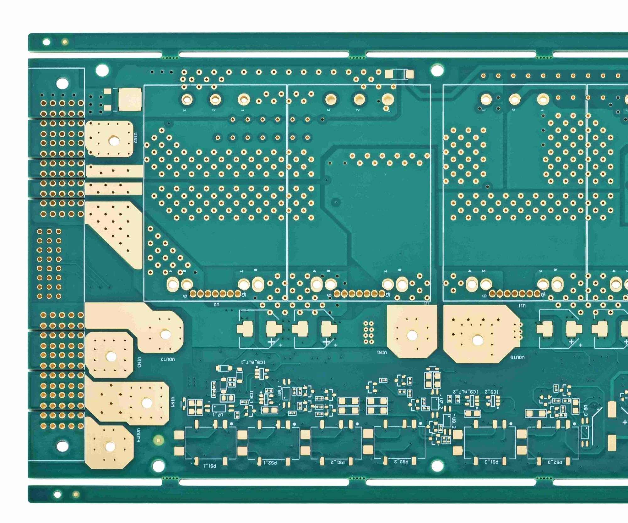
KnownPCB multilayer PCB photo from its multilayer PCB page.
Compare that layer map with the actual circuit density. If one side of the board carries most of the dense components or BGA fanout, the copper use may differ from the opposite side. That difference is an input for the stackup review. Do not try to solve it by adding copper fill before checking what the fill does to impedance and return paths. Altium’s guide to multilayer layer functions shows how signal and plane assignments depend on the intended routing.
Also identify which layers are paired with a reference plane. Altium’s multilayer-layer guide describes ground and plane layers as part of the layer-assignment decision, not as labels that can be added after routing. Keep the reference arrangement visible in the stackup and in the fabrication cross-section.
A core is a copper-clad laminate with cured dielectric between its copper layers. Prepreg is a fiberglass reinforcement coated with partially cured resin. During lamination, the resin flows and bonds adjacent layers. This difference affects the build sequence and the finished dielectric thickness. Altium’s stackup fabrication overview describes the core, prepreg and foil-lamination roles.
 Four-layer printed circuit board photographed at its edge, where copper layers are visible.](/upload/image/20261105/multilayer-pcb-edge.webp "[multilayer-pcb-edge.jpg](/users/mac/desktop/knownpcb/batch-2026-11-04-first10/media/k03/multilayer-pcb-edge.jpg) four-layer printed circuit board photographed at its edge, where copper layers are visible.")
Four-layer printed circuit board with copper visible at the edge, by Sieobserver / Christoph Kappel, shared under CC BY-SA 3.0; original file.
The edge photograph shows visible copper layers on a finished board. It does not identify the laminate grade or tell us where the core ends and each prepreg layer begins. Use the manufacturer’s stackup drawing and material names for those details.
Read the stackup from one side of the board to the other. Record the copper layers, core sections, prepreg plies and dielectric thicknesses. Check whether the material family and available thicknesses can meet the target total board thickness and impedance geometry. A typical material data-sheet value does not by itself specify the exact pressed dielectric thickness for a particular build.
The fabricator should review the material system and layer order before trace widths are treated as final. Altium’s multilayer stackup planning guide recommends choosing material and thickness with the application, electrical requirements and fabrication process in view. Its fabrication overview also explains that etching and lamination change the actual trace cross-section and dielectric spacing. These are reasons to resolve the stackup before releasing controlled-impedance geometry, not reasons to copy another board’s dimensions.
Do not add HDI lamination cycles to a standard multilayer discussion unless the via structure actually needs them. If the design uses blind or buried vias, include the hole spans and associated lamination sequence in a separate engineering review.
“Copper balance” can refer to more than one problem. The designer may be checking copper distribution across layers and across the board to reduce mechanical imbalance. The fabricator may be considering thieving to improve copper-plating uniformity. A ground fill is a circuit feature that can change the electromagnetic environment around nearby traces. Those actions are related to copper, but they are not interchangeable.
First compare the layer stack and the copper artwork. Look for large differences in copper coverage between opposing layers, uneven copper density across the panel, or a ground plane that is heavily cleared under one region and solid under another. Then ask which risk is being addressed: stackup symmetry, pressed thickness, plating distribution, or signal reference continuity.
Altium’s stackup article describes plating thieving as nonfunctional copper features that a fabricator may add to help distribute plating current in its stated process context. That does not mean the designer should add a solid ground flood near controlled-impedance traces. The same source discusses how added copper near a trace changes the electrical geometry. Before fill is added, review its net connection, clearance from signals, and effect on the reference structure.
Avoid treating the phrase “balance the copper” as a fabrication instruction by itself. If the manufacturing team proposes thieving or balancing copper, define where it may be placed, which signal layers must be protected, and whether an approval is required before the artwork changes. Preserve the released Gerber or IPC-2581 data and record the approved revision.
| Conflict found | What to check next |
|---|---|
| Copper density differs sharply between corresponding layers | Compare the actual copper artwork and cross-section, then ask the fabricator whether the pattern affects pressing or board flatness. |
| Copper fill is proposed near controlled traces | Check the reference plane and trace geometry again before approving the fill, since nearby copper can change the electrical environment. |
| Thieving is proposed for plating | Agree which layers and regions may receive nonfunctional copper and preserve clearance from impedance-sensitive routes. |
These checks address different stages. Pressing concerns the full panel and layer build. Thieving can be a fabricator-added feature for plating. Ground fill can change local impedance. The release note should name the specific issue and approved change rather than asking the fabricator to “balance copper” without limits.
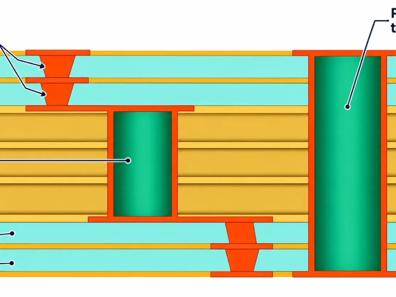
Choose the hole structure from the layer connection and the component requirement. A plated through-hole, a non-plated hole and a via have different electrical and manufacturing roles. State which layers the hole connects, whether it is plated, and whether a filled or capped via is required. For controlled routing, also show which signal layers use the hole and which barrel section is unused.
The drill table and stackup drawing must agree on the finished hole, tool size, location and plating requirement. The fabricator may need to account for the difference between a drilled hole and the finished plated opening, so do not label a finished hole as a drill diameter without saying so. Confirm the drill span against the actual board thickness and the agreed plating process.
Drill limits depend on finished board thickness, hole type, required copper and the process route. Ask the fabricator to confirm the applicable aspect-ratio and hole-size rules for this stack before selecting a small via. Use the stated diameter basis, since a drilled diameter and a finished plated opening produce different ratios.
When a drill map conflicts with the fabrication drawing, stop and reconcile the files. A fabricator should not need to infer whether the drill table or a copper layer has the final authority.
Before release, compare these items in the same revision:

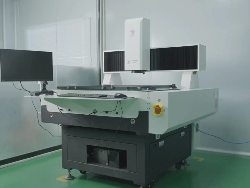
Production equipment shown on KnownPCB's multilayer PCB page.
Ask the manufacturer to confirm any item that is missing or conflicts with another file. Capture the answer in the released drawing or fabrication note so the same instruction reaches the CAM and production stages. Do not use an article, an old job example or a product-page limit to replace the current project’s approved cross-section.
For a layer-specific worked example, see the existing 8-layer PCB manufacturing and DFM guide and 8-layer PCB stackup article. For a manufacturing quote, use the multilayer PCB page or contact KnownPCB.
October/20/2026HDI PCB Manufacturer Evaluation: Prove the Build
February/25/2026Rigid-Flex PCB Benefits: Space and Reliability
October/15/2026Stacked vs. Staggered Microvias: Choose by Constraint
November/05/20266-Layer PCB Stackup: Routing and Reference Planes

September/06/2026High Current PCB Design: Current Paths, Copper, Vias & Thermal Limits
Proven by 7 industries, 4000+ customer projects
Please contact us at sales@knownpcb.com, ask for engineering support here or use the form below to reach out to KnownPCB | Request a Manufacturing QuoteInclude your quantity, target delivery date and key requirements. File handling and NDA information. |