
Blog & Design Guide

A 6-layer PCB stackup can be arranged to leave more copper layers available for signals or to give power and ground more dedicated layers. The right choice depends on signal count, power delivery, reference continuity, impedance needs and component placement. No single layer order is the best fit for every six-layer board.
The two options below are design examples from Altium’s six-layer stackup guide. Use them to compare routing space and plane coverage, then work with the fabricator to confirm the finished cross-section. They are not a KnownPCB standard stackup.
On this page
Before assigning the six copper layers, list the interfaces that need controlled impedance, the number of signal routes, the power rails, and the ground references each signal will use. Also identify where components sit on the top and bottom sides. These details determine whether the design can make use of internal signal layers or needs more plane coverage.
For a fast interface, mark the signal route and reference conductor together. A signal layer without a nearby reference plane may still be usable, but the return route and impedance geometry need a clear review. Texas Instruments’ high-speed layout guidance calls for high-speed routes to use a continuous ground reference. Altium’s six-layer examples likewise tie layer assignment to the design’s routing, power and EMC needs.
Altium’s examples show different ways to spend the six copper layers. The first keeps more room for signal routes, while the second assigns more layers to ground and power. The board photo below shows two boards that the NyanSat project identifies as six-layer boards. A surface photo does not reveal their internal layer order, so use the released cross-section, not the appearance of a board, to confirm a stackup.
 Two NyanSat printed circuit board assemblies, the Combined Payload Board and the Obi Wan Komputer.](/upload/image/20261105/nyansat-cpbobc.webp "[nyansat-cpbobc.png](/users/mac/desktop/knownpcb/batch-2026-11-04-first10/media/k04/nyansat-cpbobc.png) two nyansat printed circuit board assemblies, the combined payload board and the obi wan komputer.")
NyanSat's Combined Payload Board and Obi Wan Komputer, by Oakwood Engineering, shared under CC BY-SA 4.0. The project identifies both as six-layer boards; source and license.
One signal-rich example uses this order from the top surface to the bottom:
SIG+PWR / GND / SIG / SIG / GND / SIG+PWR
The surface layers carry signals and may also carry power rails or copper pours. Ground planes on L2 and L5 provide references for surface routing. The two inner signal layers add routing space. In Altium’s example, the inner routes are better suited to lower-speed signals, while higher-speed routes remain on the outer layers near their ground references.
This option can help when signal routing space is the main constraint. It does not create a dedicated internal power plane pair, so the power-distribution network and return path must be checked carefully. The designer should also watch the reference geometry around split power copper and ensure a high-speed route never depends on an interrupted plane.
The pattern pairs signal-plus-power surface layers, two ground references, and two inner signal layers. If the inner signals run side by side, review their routing directions and coupling. A signal assignment is only useful when the selected reference and dielectric spacing are recorded for that layer. Any final trace width still depends on the confirmed material, copper and finished cross-section.
A plane-focused example in Altium’s EMC article uses this order:
SIG / GND / PWR / GND / SIG / GND
This arrangement leaves two layers mainly for signals and three for ground, with one internal power plane. It can provide more shielding and power distribution options than Option A. It also reduces the number of layers available for signal routing. Altium’s six-layer EMC examples note that the bottom ground layer can limit component placement or routing on that side unless the layout has suitable clearances.
Do not assume the power plane is a suitable high-speed reference. TI’s guidance for high-speed interfaces prefers a continuous ground reference. If a signal uses a layer adjacent to the power plane, its reference and return route need explicit review. A power-plane split or a transition between reference regions may change the return path.
This plane-focused option may suit a board that needs more ground coverage and a defined power layer, but it can constrain bottom-side component access. The allocation also needs a mechanical review. Compare the copper function on each layer with the dielectric build on the opposite side, then ask the fabricator to confirm the cross-section and any copper-distribution changes before routing begins.
The table summarizes the tradeoff. Actual geometry still depends on the board design.
| Decision | Option A | Option B |
|---|---|---|
| Routing layers | More signal-routing space, including two inner signal layers. | Fewer signal layers, with one power plane and more ground coverage. |
| Power delivery | Power rails share surface signal layers. | One internal power layer can carry defined power regions. |
| Reference review | Keep fast outer routes over continuous ground. Review how inner routes return to ground. | Keep high-speed routes referenced to continuous ground. Do not assume the power plane is a ground substitute. |
| Main constraint | Power distribution and reference continuity need more attention. | Routing space and bottom-side component placement are tighter. |
For each critical route, identify the reference layer before and after a signal via. If the route changes layers, check whether its ground reference remains continuous. If it moves between ground regions, add an intentional connection between those ground regions near the signal transition where the design requires one.
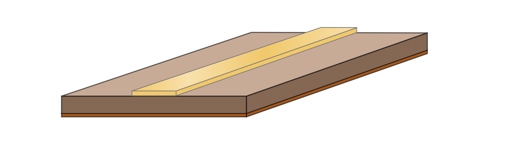
Microstrip structure diagram by Spinningspark, shared under CC BY-SA 3.0; original file.
A split in a reference plane can force the return current to detour and can change the signal loop. Texas Instruments’ High-Speed Interface Layout Guidelines discusses this problem in section 2.4 and shows a stitching arrangement for a particular high-speed interface. That placement example is not a universal six-layer via rule. Check the actual plane geometry and the signal transition before routing.
A power plane may carry a supply rail and may be split into separate regions. Before placing a fast route next to it, confirm whether the signal uses that plane as its reference or whether it is referenced to ground on another layer. If a signal changes reference regions, show where the return current crosses between those regions.
The illustration shows a microstrip and ground vias connected to a ground plane. It does not depict a power-plane split or a transfer between different reference nets; check those conditions in the actual stackup.
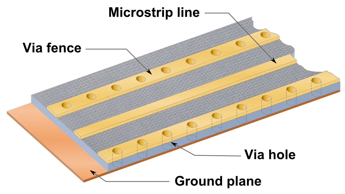
Via fence in microstrip, by Spinningspark, with background texture from Agnellous's public-domain Fibreglasscast.JPG. CC BY-SA 3.0; original diagram.
Check a split or cutout against the plane that actually references the signal. A route crossing a split in its reference plane requires review of the return-current connection. A route referenced to continuous ground is a different case. A split in a non-reference power plane is not automatically a routing prohibition. Use a stitching capacitor only where the circuit and signal-integrity review require the relevant reference-transfer path.
After choosing a layer allocation, confirm the finished material stack before routing impedance-controlled traces. The dielectric thickness between a trace and its reference plane, copper weight, trace width and spacing all affect the cross-section. Altium’s six-layer design guide covers these choices as stackup and routing decisions. If the fabricator changes a material or dielectric thickness, recalculate the geometry before releasing the board.
Finished board thickness and local dielectric spacing are different measurements. The total thickness is the sum of copper, laminate, prepreg and other layers in the cross-section. The spacing from a signal trace to its reference plane is only one part of that build. Record each value against its layer pair so a reviewer can check the intended impedance without guessing which thickness applies.
The release package should name every copper layer and its role. Include the material family, dielectric thicknesses, copper weights, controlled-impedance definitions, drill table and via spans. If you have a high-speed transition, state which plane references it and whether any backdrill is required. Do not write “standard six-layer stackup” when the design actually requires a specific layer order.
For every critical signal, check its source and destination layers, the reference plane along each segment, and the return connection at a layer change. Check that a ground reference has not been split under the route. If a signal must cross a reference boundary, document the intended return connection and review it with the signal-integrity owner. TI’s high-speed layout note shows a stitching arrangement for a specific interface; it is a starting example, not a universal via spacing rule.
Altium’s six-layer routing examples are useful starting points for comparison, but the selected board still needs a project-specific DFM review. Check whether the stack is physically balanced, whether the power and ground planes meet the load needs, and whether each fast signal retains its ground reference.
For an eight-layer comparison, see the existing 8-layer PCB stackup guide. The separate PLC PCB design guide discusses PLC-specific six-to-eight-layer use. For manufacturing details, consult KnownPCB’s multilayer PCB page or contact KnownPCB.
October/13/2026Prototype to Low-Volume PCB: Bare-Board Release Gates
April/15/2026The Electrical Role of HDI Stackup
February/03/2026Type of PCB Edge Connectors Overiew

May/13/20268 Layer PCB Manufacturing and DFM Guide

September/06/2026High Current PCB Design: Current Paths, Copper, Vias & Thermal Limits
Proven by 7 industries, 4000+ customer projects
Please contact us at sales@knownpcb.com, ask for engineering support here or use the form below to reach out to KnownPCB | Request a Manufacturing QuoteInclude your quantity, target delivery date and key requirements. File handling and NDA information. |