
Blog & Design Guide

A PCB fabrication drawing tells the bare-board fabricator which construction and mechanical requirements belong to the released design. It should identify the board revision, layer build, hole data, outline, finish and any required fabrication notes. The drawing works alongside the Gerber, drill and other approved files. It does not replace them.
The main review task is consistency. The drawing, stackup, drill chart and exported layer files must describe the same board. If a note or dimension conflicts with the data, the fabricator should ask for a decision rather than guess which source controls.
On this page
Start with the board name or part number and the design revision shown in the drawing package. State the units used for dimensions. If a coordinate origin is important to the outline or drill positions, show it clearly and keep it consistent with the associated manufacturing data.
A drawing can include a title block, a view of the finished outline and notes that point to the controlling design files. The exact title-block fields depend on the company's release process, so do not treat a particular template as a universal standard. What matters is that a reviewer can tell which board the drawing describes and which revision must be compared with the Gerber and drill files.
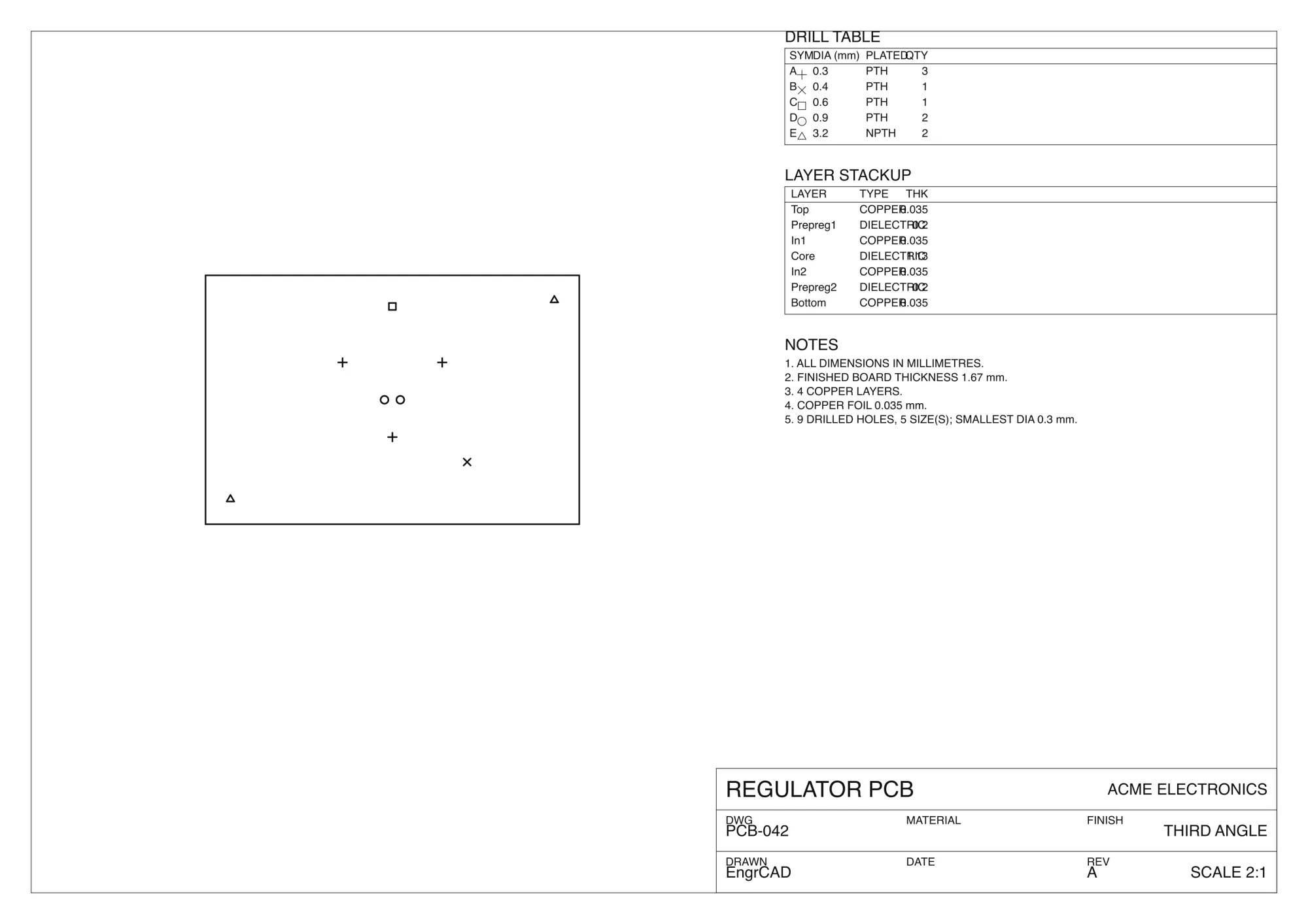
Illustrative fabrication drawing from EngrCAD documentation. © Chris Lane, MIT licensed; source SVG.
Open the full-size drawing to read dimensions and fabrication notes.
Keep bare-board construction separate from assembly instructions. The fabrication drawing describes the board itself. Component reference designators, pick-and-place locations and soldering instructions belong to assembly documentation unless they identify a mechanical feature that changes the bare board. Altium's documentation overview distinguishes fabrication data from assembly files and describes checking the design package before release.
List the conductive layers in their finished order and use the same names that appear in the design files. If the fabrication drawing calls a layer “GND2” while the Gerber set calls it “L4,” a fabricator may have to infer the relationship. Make the mapping explicit instead of relying on a page image alone.
The stackup information should identify the construction the designer intends to receive. Depending on the board, that can include layer count, layer names, core and prepreg arrangement, copper designation, dielectric spacing, finished board thickness, material requirement and surface finish. Include only values that have been selected and approved. Do not fill an open field with a typical value from an old drawing.
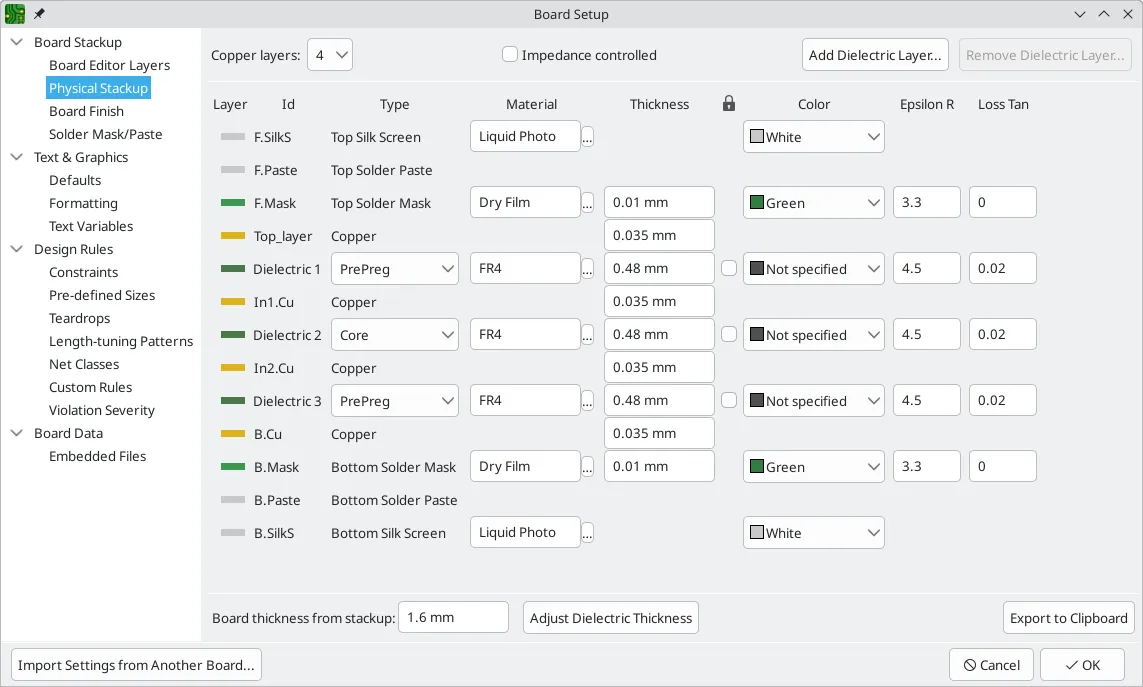
Physical stackup settings screenshot from the KiCad PCB Editor manual, licensed CC BY 3.0.
Open the full-size stackup settings screenshot to read its fields.
If controlled traces are present, tie the geometry to its signal layer and reference layer. The drawing or related stackup note should state which construction is being used. A general impedance target alone does not identify every layer's dielectric spacing or the copper build. The Altium fabrication-drawing example shows how layer images, stackup information and impedance requirements can be displayed together.
A drill chart should let a reviewer distinguish the hole categories used in the board. Give each drill symbol a matching tool size and quantity, and identify whether the hole is plated or non-plated. If the design includes blind or buried connections, state the applicable layer span in the controlled drill or stackup data.
Hole dimensions need a clear meaning. A drill tool diameter, a finished plated-hole diameter and a tolerance are different entries. Use the drawing and drill-file conventions approved for the project. Do not apply a fixed copper-plating allowance to convert between them unless the project specification explicitly defines that method. The finished requirement and the fabricator's process definition must agree.
The screenshot shows drill-file export options rather than a completed hole table. Compare the exported drill data with the approved drawing to confirm tool sizes and hole counts.
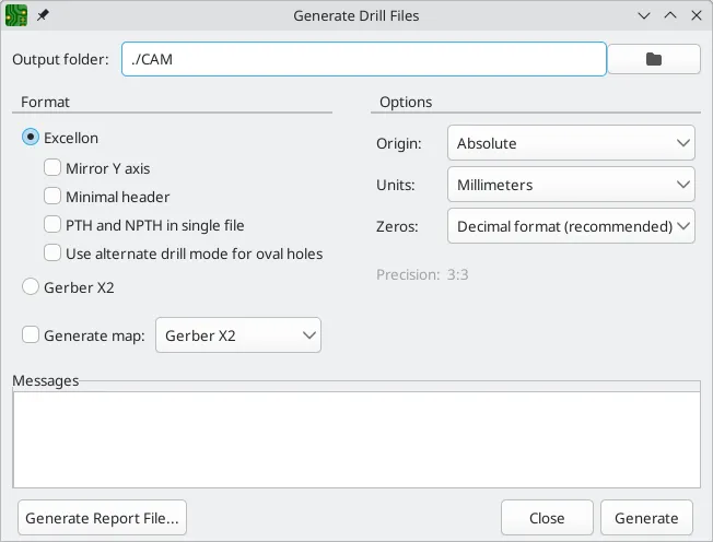
Drill-file settings screenshot from the KiCad PCB Editor manual, licensed CC BY 3.0.
Open the full-size drill-file settings screenshot.
Check that the chart's symbols match the drill data and the drawing view. The position, quantity and coordinate basis should not contradict the NC drill output. Altium's drawing guide describes symbol-based drill views and tables, but the actual finished size and tolerance must come from the approved design requirements rather than from a software example.
State the surface finish and solder-mask requirements that apply to the bare board. Show the board profile, cutouts, slots, edge details and dimensions needed to manufacture and inspect the finished outline. A visual rendering can help explain the shape, but it should not be the only source of a required dimension.
Use a note when it resolves a real manufacturing question. Examples include a local dimension, a defined edge treatment, or a feature that must remain unchanged during CAM review. Keep each note tied to the affected layer or region. A broad instruction such as “build per industry standard” does not tell a fabricator which requirement applies to this board.
List acceptance or inspection requirements only when the product team has selected them. Do not assume that a material name, finish name or drawing symbol proves a particular test result. If a requested report or special test is not part of the approved order, mark it as an open decision rather than implying it is included.
Before release, compare the drawing with the current Gerber layers, NC drill data, stackup, outline and netlist where applicable. Confirm that the revision is the same across the file set. Layer labels should agree, drill symbols should map to the right sizes and the outline shown on the drawing should match the profile data.
When two sources conflict, stop and request a written correction from the design owner. Do not let a quotation, CAM note or previous revision silently become the new design authority. Record which file changed and recheck any affected layer, hole, outline or finish note before the package is released.
The existing bare-board RFQ checklist covers how to compare quotes using one controlled data package. The prototype-to-low-volume release guide covers revision gates for a later lot. For multilayer manufacturing context, see the multilayer PCB page. Use the contact page when the drawing or file set needs a manufacturing clarification before release.
October/27/2026PCB Differential Pair Skew: Convert Time to Length
September/01/2026LED Aluminum Core PCB Design to Manufacturing
November/05/20266-Layer PCB Stackup: Routing and Reference Planes
March/26/2026What Is an Embedded Copper coin PCB and When Should You Use It?
March/30/2026The Definition of Through Via, Blind Via, Buried Via
Proven by 7 industries, 4000+ customer projects
Please contact us at sales@knownpcb.com, ask for engineering support here or use the form below to reach out to KnownPCB | Request a Manufacturing QuoteInclude your quantity, target delivery date and key requirements. File handling and NDA information. |