
Blog & Design Guide

Choosing a PCB material for high speed design starts with the channel loss budget, operating frequency, route length and stackup. A laminate name alone cannot show whether the finished construction will meet the electrical requirement. The material choice also depends on signal geometry and mechanical conditions.
Start with the interface and its route, then compare the material data that affects that route. The data should match the measurement conditions and the construction being considered. The final request to the fabricator should identify both the material evidence and the stackup that must be built.
On this page
Record the signal interfaces that drive the board's speed requirements. Include the frequency range or edge-rate context used by the design team, the route length, the layer arrangement and the loss margin available to the channel. A short path with comfortable margin may not need the same dielectric choice as a long path with limited margin. The material decision begins with that use case, not with a catalog label.
Line geometry and layer thickness also affect the decision. A change in dielectric constant or dielectric thickness changes the field around a trace and may require a different width or spacing to preserve the target impedance. A material choice must therefore be checked against the proposed stackup and routing geometry. Do not treat a datasheet value as if it described every line structure on the board.
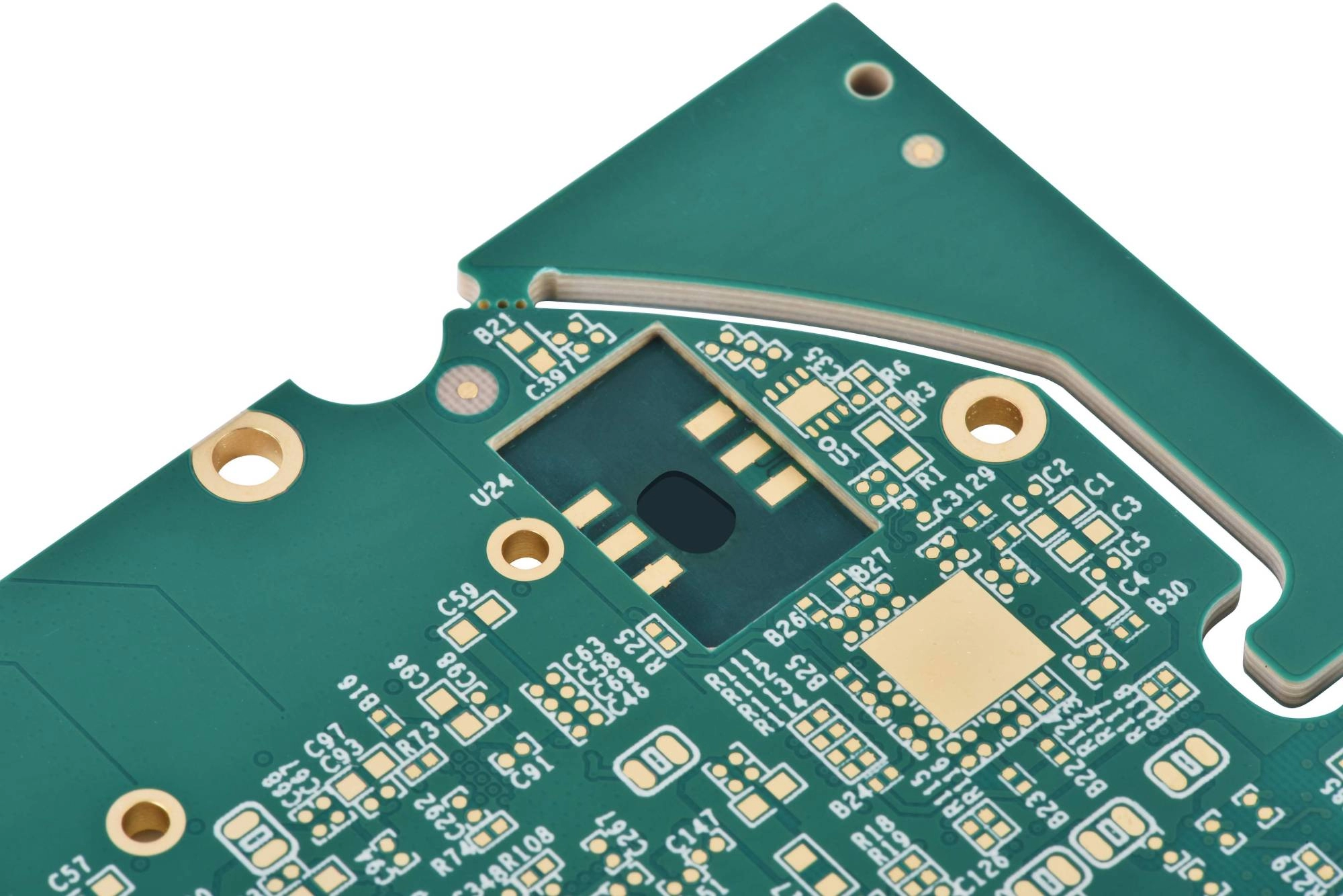
KnownPCB high-frequency PCB photo from its high-frequency and high-speed PCB page.
Begin with the construction already assumed in the design and ask what evidence shows it is sufficient. If the loss budget is tight, examine the dielectric and conductor contributions before changing a material family. If the budget has margin, a lower-loss option may not justify its effect on board cost or build complexity. Altium's high-speed stackup discussion also treats material as one part of the complete stack and geometry decision.
Dk describes the dielectric response used in the electrical model. Df, often called loss tangent, describes a component of dielectric loss. The values depend on the material construction and measurement conditions. Two data-sheet values should not be compared as if they were measured at the same frequency and with the same method when the documents say otherwise.
Check the frequency, test method, laminate construction, resin content, thickness and copper configuration listed with the data. Then connect those conditions to the signal layer and expected field structure. A published Dk or Df without its test conditions is not enough to select a stackup. Altium's material-selection overview describes the properties to compare and why the values must be read in the context of the material and frequency.
Do not choose the lowest Dk as a universal goal. Dk and thickness affect impedance geometry and propagation, while Df relates to dielectric loss. The useful balance depends on the channel, layer count, routing width and the product's mechanical requirements. The material data must fit the full set of constraints.
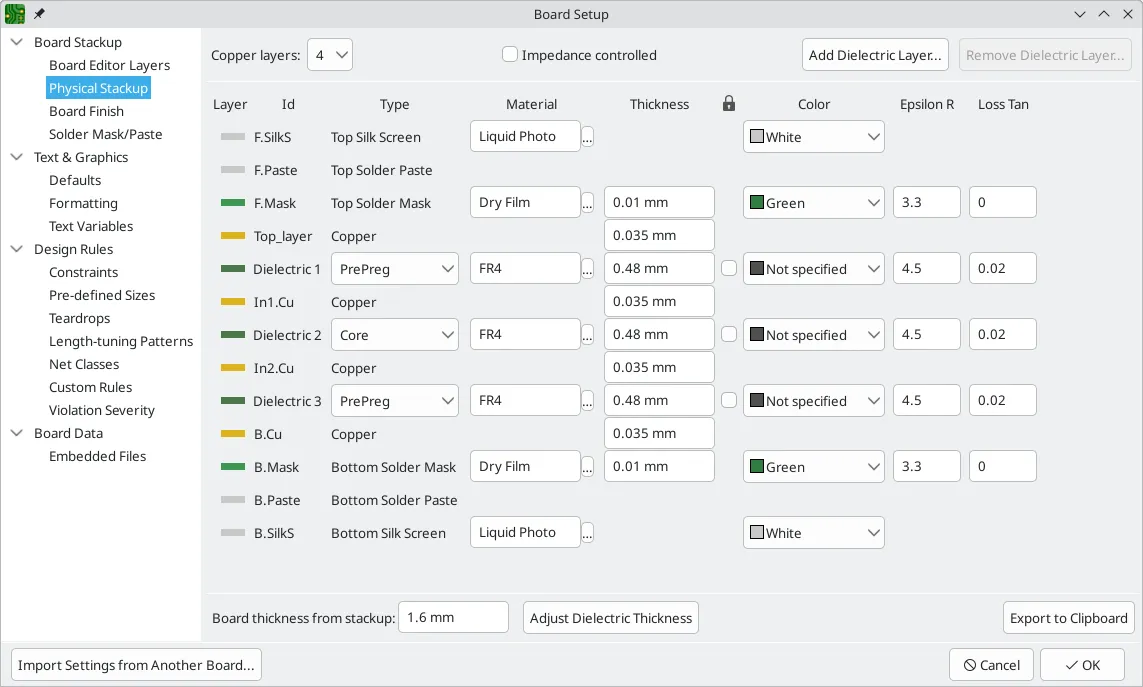
KiCad physical stackup settings screenshot from the official manual, licensed CC BY 3.0. The displayed FR-4 values are software example inputs, not a generic FR-4 specification or KnownPCB measurement; no test frequency or method is shown.
Open the full-size material-field screenshot to read its inputs.
The dielectric is only one part of a high-speed transmission line. Copper foil type and the surface facing the dielectric also affect conductor loss. Ask for the foil designation and any roughness metric the material supplier reports. Confirm that the data refers to the same copper surface and construction that will appear in the finished board.
Do not reduce copper roughness to one number without recording how it was measured. Different roughness parameters and measurement methods are not interchangeable. The existing copper roughness and skin-depth article explains those measurements and the limits of the simplified loss model.
Glass style, weave and resin content also belong in the stackup discussion. The reinforcement and resin affect the dielectric system and can change the material properties seen by a routed line. Ask which construction is proposed, not only which resin family or laminate brand is named.
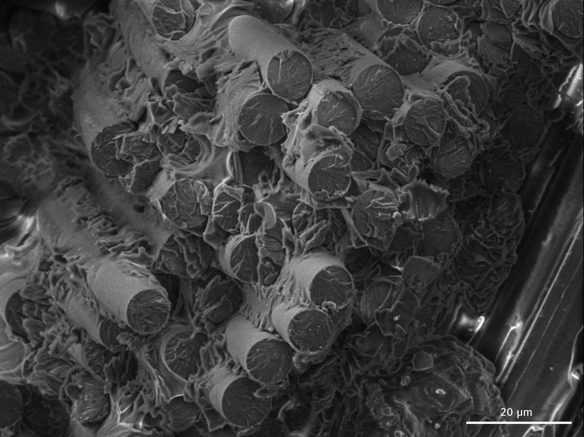
PCB cross-section micrograph by ZEISS Microscopy from Wikimedia Commons, shared under CC BY-SA 2.0.
A material that looks attractive in a data sheet still has to work in the finished board. Check the target thickness, number of layers, copper type, layer position, bonding construction and drill structure together. A thinner dielectric may support a compact build, but it also changes the required trace geometry. A low-loss choice is useful only when it fits the layout and can be made to the approved construction.
Include thermal and mechanical conditions in the comparison when they affect reliability. Tg and CTE are not substitutes for dielectric loss data, and a high Tg does not prove that the material meets a signal-loss target. If the design's main question is Z-axis expansion and via-barrel strain, use the separate CTE and via-strain article rather than repeating its calculations here.
When comparing named laminate grades, review the exact data sheet, construction and substitution limits. The existing RO4350B versus RO4003C comparison shows how a grade comparison can be made without assuming that two similar names are interchangeable.
A useful material request connects the product requirement to the data the fabricator can review. Include the frequency range, channel loss target or margin, controlled layers, routing geometry, required finished thickness, copper configuration and allowed material substitutions. Name the source and revision of the data sheet used in the design review.
| Design question | Material information to compare | Release check |
|---|---|---|
| Where is the channel loss margin tight? | Df and dielectric test conditions at the relevant frequency, with the intended route length. | Confirm that the cited data matches the chosen construction and line structure. |
| Does the stackup support the required geometry? | Dk, dielectric thickness, copper and layer position. | Check the proposed dimensions against the released stackup and fabricator review. |
| Can conductor loss be compared fairly? | Foil type, surface treatment and the reported roughness method. | Record which copper surface faces the dielectric and link the full roughness analysis when needed. |
| Will the board survive its environment? | Glass/resin construction and the relevant thermal or mechanical data. | Compare the board's service conditions without treating Tg or CTE as loss metrics. |
Ask the fabricator to confirm the exact construction, layer locations, copper and bonding system before release. If an alternative material is proposed, return the changed data for electrical and mechanical review. A generic “equivalent” note does not show whether the new construction meets the same channel requirement.
KnownPCB's high-frequency and high-speed product page provides the service context. Use the contact page to submit the stackup and material requirements for a manufacturing discussion. These links do not imply that any particular laminate is in stock or approved for an unreviewed design.
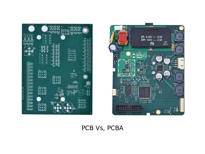
June/12/2026PCB Vs PCBA: Differences, Definitions and Relations
April/14/2026Industrial PCB Design Features
April/16/2026High-Current Heavy Copper Design & Manufacturability
October/22/2026MCPCB Thermal Resistance: Specify the Heat Path
October/21/2026Flex PCB Supplier Evaluation: Check the Construction
Proven by 7 industries, 4000+ customer projects
Please contact us at sales@knownpcb.com, ask for engineering support here or use the form below to reach out to KnownPCB | Request a Manufacturing QuoteInclude your quantity, target delivery date and key requirements. File handling and NDA information. |