
Blog & Design Guide

High-speed PCB design starts with the electrical behavior of an interface, not with one universal clock-rate cutoff. Edge rate, trace delay, route length and the chosen stackup determine when a trace must be treated as a transmission line. The manufacturing review then asks a practical question: does the released stackup keep a clear reference path as each signal crosses the board?
This guide follows that path from interface definition to layer transition and fabrication notes. It focuses on return-path continuity across layers. It leaves detailed skew and residual-stub calculations to the related articles.
On this page
Begin by identifying the signals that need controlled impedance or a specific return path. A board may carry slow control signals, fast memory or serial links, and analog or RF nets at the same time. Assigning every net the same routing treatment can use layers without solving the actual signal-integrity problem.
For each interface, record the driver and receiver, the signal class, the target impedance if specified, the route length that matters, and the layer or plane intended to provide the reference. Altium describes edge rate as a useful way to identify high-speed digital behavior because fast signal transitions can make a line electrically long even when its data rate alone seems modest. This is a design screen, not a substitute for the interface specification or a channel analysis. Altium’s high-speed design overview explains the role of edge rate, stackup, interconnect and routing.
Next, map each controlled signal layer to its reference conductor. A surface microstrip may use the adjacent ground plane. An internal stripline may be bounded by reference planes on both sides. Record the dielectric layer and the reference plane in the stackup table instead of leaving the fabricator to infer them from a schematic or a net name.
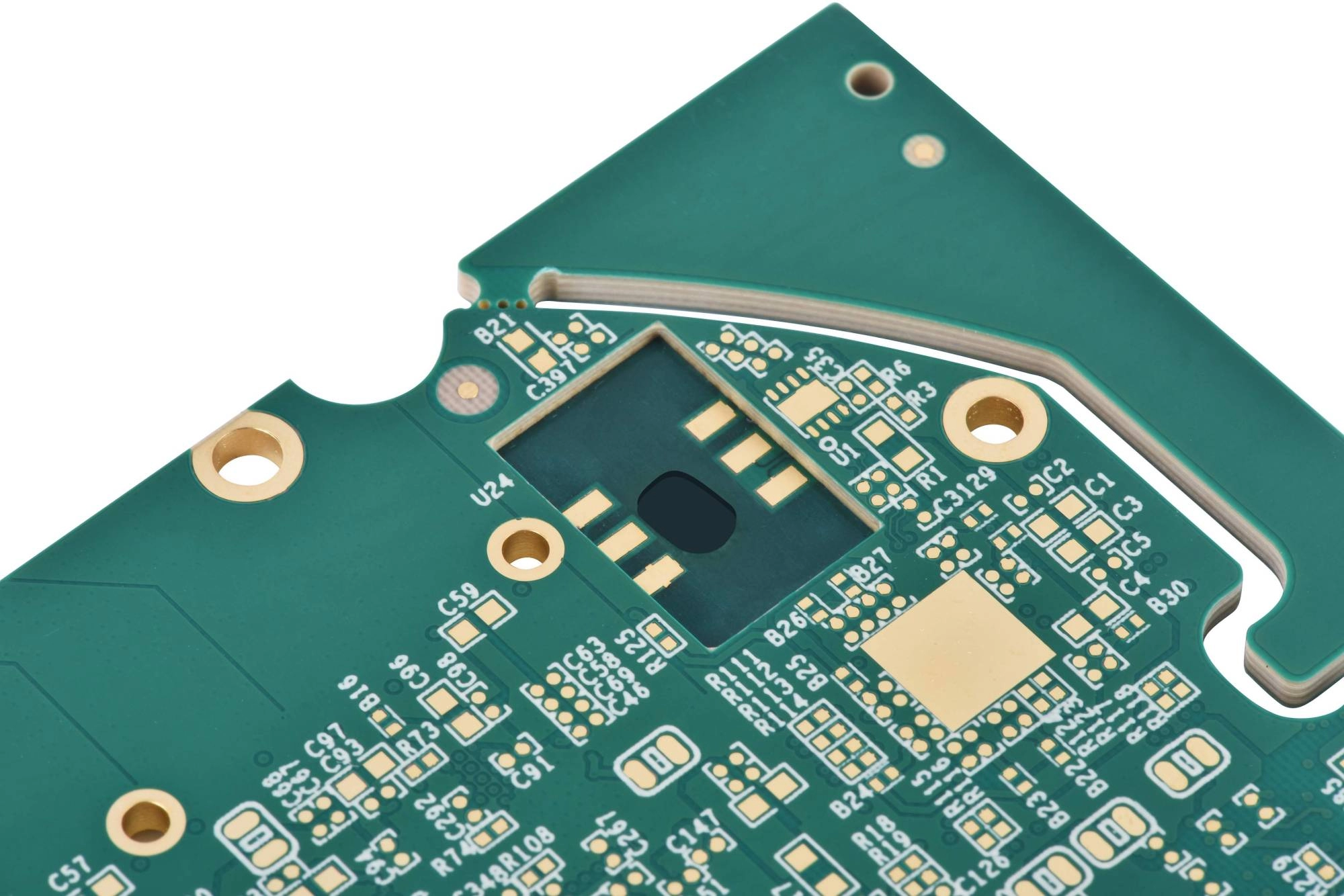
KnownPCB high-frequency PCB photo from its high-frequency and high-speed PCB page.
A signal layer assignment should also fit the routing density. If a bus needs many routes and vias, it may require more signal layers. If a layer is reserved for a reference plane or a power distribution network, note what that choice does to the remaining routing space. The number of copper layers alone does not say whether the design will maintain its target impedance or keep a continuous return path.
A signal current has a return current. At high frequencies, the return tends to follow the path that keeps the loop impedance low and stays close to the signal route. A continuous ground plane gives the return current a defined path under a surface trace or between the reference planes of an internal trace.
A split, void or large opening in that reference plane changes the path. The return current must go around the obstruction or use another connection. That detour increases loop area and can change coupling, emissions and signal behavior. TI’s High-Speed Interface Layout Guidelines discusses these effects in section 2.4. Its examples apply to the interface conditions in that note, but the review question is useful for any controlled signal: does the assigned reference conductor continue beneath the route?
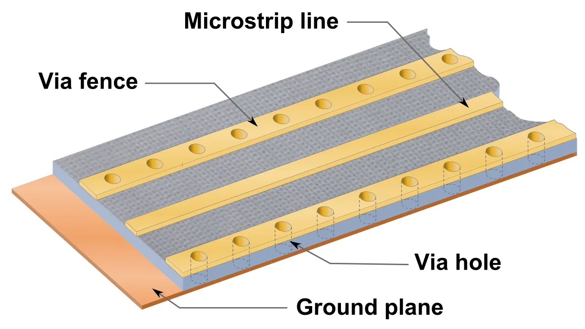
Via fence in microstrip, by Spinningspark, with background texture from Agnellous's public-domain Fibreglasscast.JPG. CC BY-SA 3.0; original diagram.
When a route must pass near a plane cutout, first check whether the route can move to a layer with an uninterrupted ground reference. If the crossing cannot be avoided, the design team must provide an intentional return connection, such as an approved stitching capacitor across a split where that is electrically appropriate. Do not assume that copper fill will bridge the electrical gap. The fill must be connected and placed according to the released circuit design.
Keep the return-path review tied to the actual layer stack. A power plane may carry a DC supply, but that does not make it a suitable reference for every high-speed net. TI’s guideline prefers a solid ground reference for the high-speed signals it covers. If a signal moves between reference planes, document whether they are the same ground network and how the return current stays continuous.
A signal via changes the conductor geometry and can create an inductive or capacitive discontinuity. The return current also needs a path as the signal changes layers. If the signal goes from a layer referenced to one ground plane to a layer referenced to another, those ground regions need a nearby connection that suits the board’s stackup and frequency range.
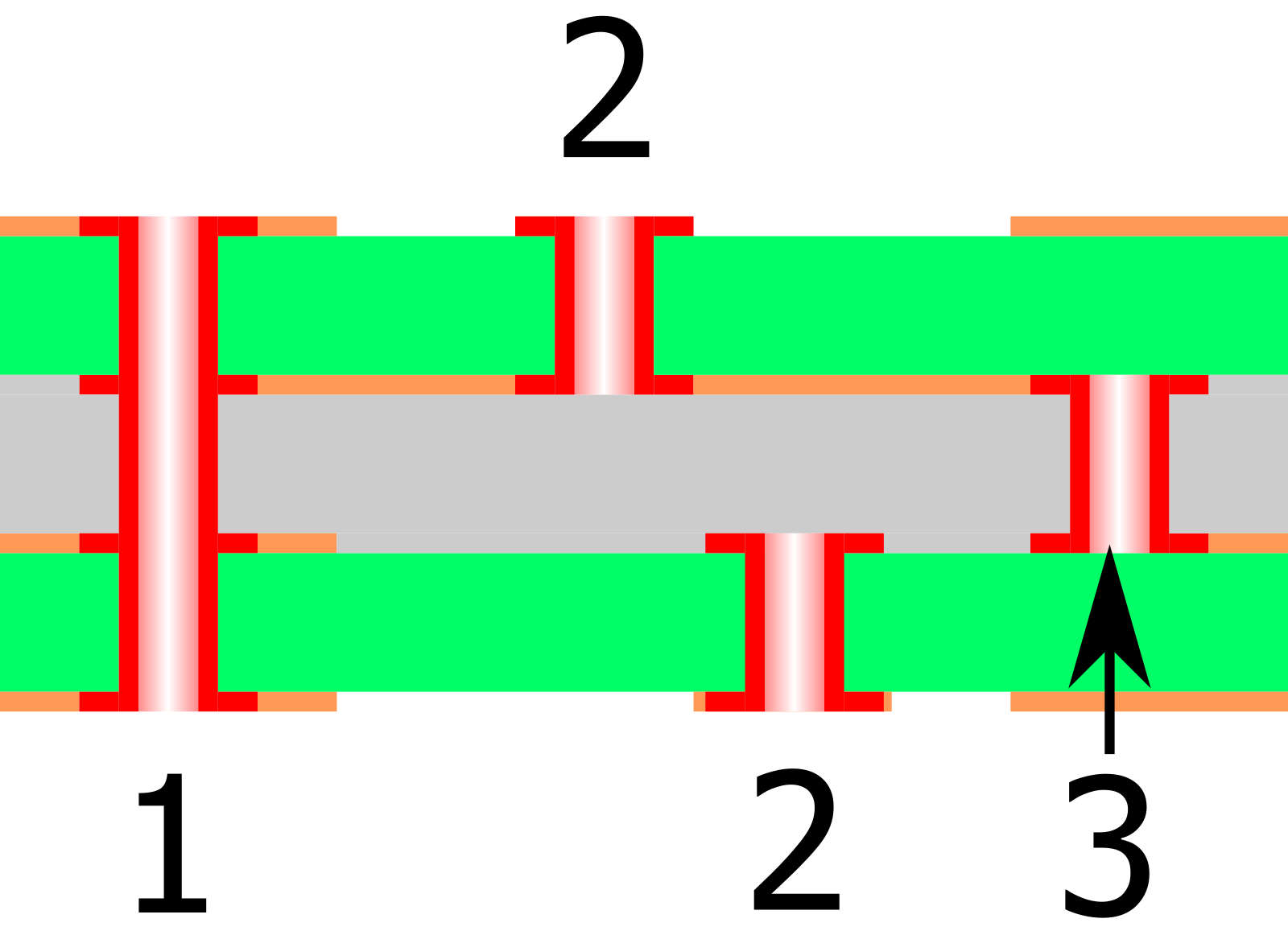
PCB via types diagram by M. Adler, shared under CC BY 3.0; original file.
Review the transition as a pair of current paths. For each signal via, record the start layer, end layer, hole type, and reference plane before and after the change. Then show how the return current moves between the two references. Where the return planes are separate, the layout may need a ground stitching via close to the signal via. The location should follow the actual plane geometry and the interface design, not a blanket grid rule.
TI’s SPRAAR7J note shows stitching vias placed symmetrically within 200 mils center to center of the signal transition via in its ground-reference transition example, with closer placement preferred. Treat that as an example from the named high-speed routing guideline, not as a universal fabrication tolerance. The same note says to keep the signal on a continuous ground reference where possible and to review both the signal and return paths at a layer change.
Also check whether the signal via crosses unused layers and leaves a stub beyond the destination layer. A stub is another part of the transition geometry. Its electrical effect depends on its length and the signal spectrum, so the design team should state the layer span and any required backdrill from the approved stackup. The existing backdrill residual-stub guide covers the depth datum, tolerance chain and residual-stub review.
Do not add backdrill instructions to every via simply because a board is called high speed. First identify which through vias connect to an internal layer and which signal paths leave a meaningful unused barrel. The selected stub length, backdrill depth, drill diameter and remaining dielectric all depend on the board cross-section and process plan.
For differential interfaces, check both conductors as a pair. Their layer spans, via counts and escape geometry should stay consistent with the interface rules. If a time-matching problem remains, use the separate differential-pair skew guide. Do not replace a measured timing budget with a generic length target.
The fabrication drawing should distinguish the original drill from any secondary backdrill, identify which side the backdrill starts from, name the target layer, and include the allowed depth and residual-stub requirement. The manufacturer can then check the notes against the finished layer stack and the available drill sequence. If those values are not agreed, stop the release and resolve them before the board is built.
Before releasing the files, compare the PCB data, the stackup cross-section and the fabrication notes. Use a short transition table for every critical interface:
| Item | What the release package should state |
|---|---|
| Signal route | Interface name, start and end layers, impedance target if specified, and any required matching rule. |
| Reference path | Ground plane for each signal segment and how the return remains continuous at a plane change. |
| Signal via | Via type, drill data, layer span and any required backdrill or via fill. |
| Cross-check | Agreement among the stackup, Gerber or IPC-2581 data, drill table and fabrication notes. |
If the stackup changes after impedance or routing work has started, recheck the affected trace geometry and via transitions. A new dielectric thickness or plane arrangement can change both impedance and the return-current path. Do not preserve an earlier trace width by habit when the cross-section has changed.
For manufacturing support, send the released stackup, drill table and transition requirements with the design files. See KnownPCB’s high-frequency and high-speed PCB manufacturing page or contact KnownPCB for a quote.
October/26/2026PCB Copper Thickness: Ounces, Microns and Resistance
July/23/2026PCB Common DFM Mistakes and Solutions

May/12/20266 FPC Design Details to Prevent Assembly Failures
October/13/2026Multi-Design PCB Panelization: IDs and Revisions
May/21/20268 Layer PCB Stackup:Headache Design Problems and Cost
Proven by 7 industries, 4000+ customer projects
Please contact us at sales@knownpcb.com, ask for engineering support here or use the form below to reach out to KnownPCB | Request a Manufacturing QuoteInclude your quantity, target delivery date and key requirements. File handling and NDA information. |