
Blog & Design Guide

RF PCB design needs a defined signal conductor and a connected return structure from the device port to the end of the route. A line can have the intended width while a ground gap, a disconnected top-side pour, or a poorly described layer change interrupts that structure. Before fabrication, review the ground connections and local geometry together with the signal artwork.
The useful manufacturing handoff follows the RF path. It identifies the reference plane beneath each section, where ground changes layers, which geometry belongs to a connector or device footprint, and which features must remain unchanged during CAM preparation. Start with that path rather than treating every isolated clearance as an independent rule.
On this page
Mark the route between its actual electrical endpoints. An RF IC pad, matching network, filter, connector and antenna feed can require different local structures. The package recommendation may include a short neck, a grounded pad, or a deliberate change in clearance. An antenna region can have its own copper keepout. Record those exceptions so that a general ground-pour operation does not overwrite them.
State the operating band and identify any sensitive receive or high-power transmit path. A digital control line on the same board introduces an additional routing problem, but it does not make every trace an RF transmission line. Keep the RF region, noisy switching circuits and digital connections visible in the review data. The fabricator needs to know which copper features are electrically intentional.
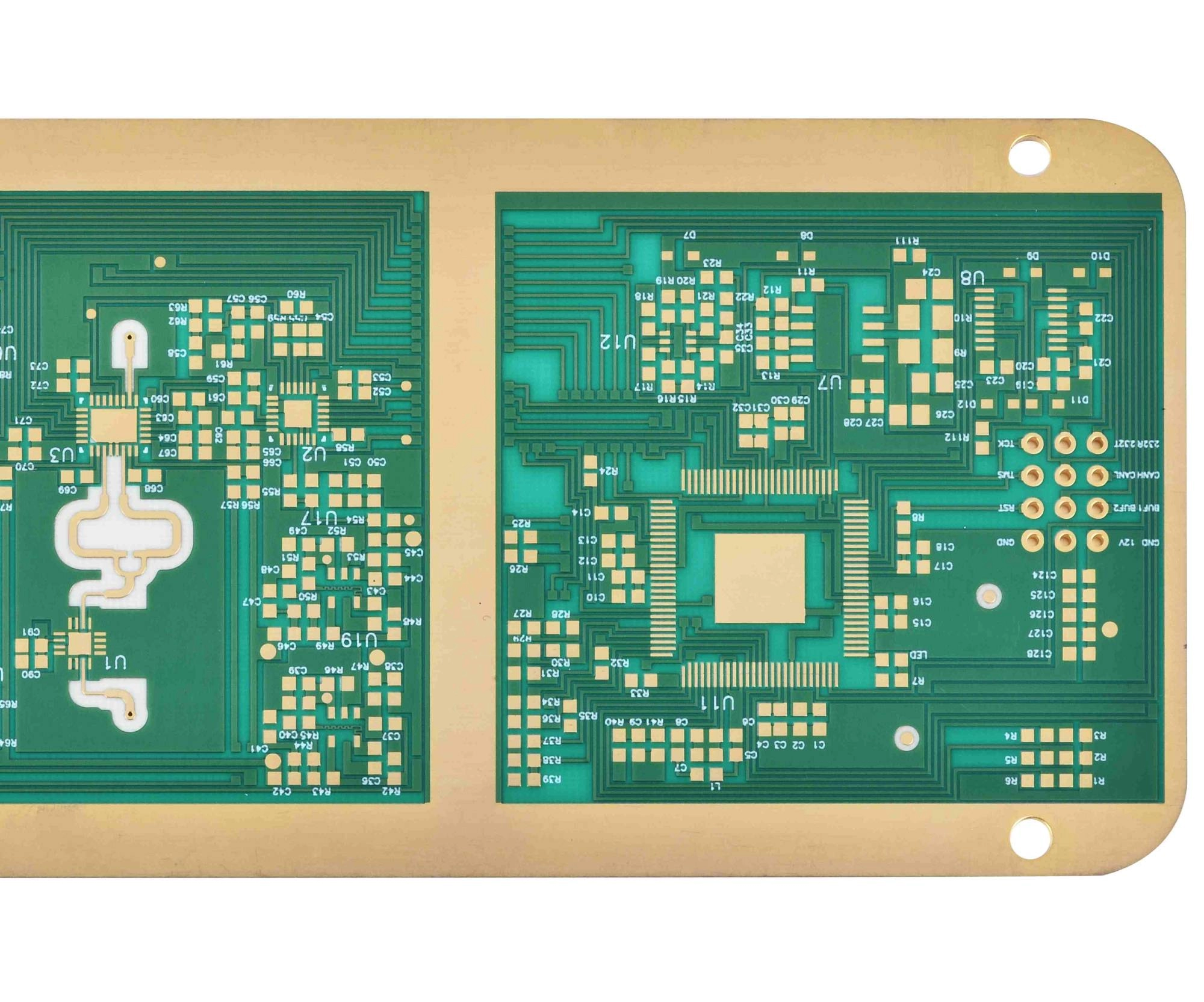
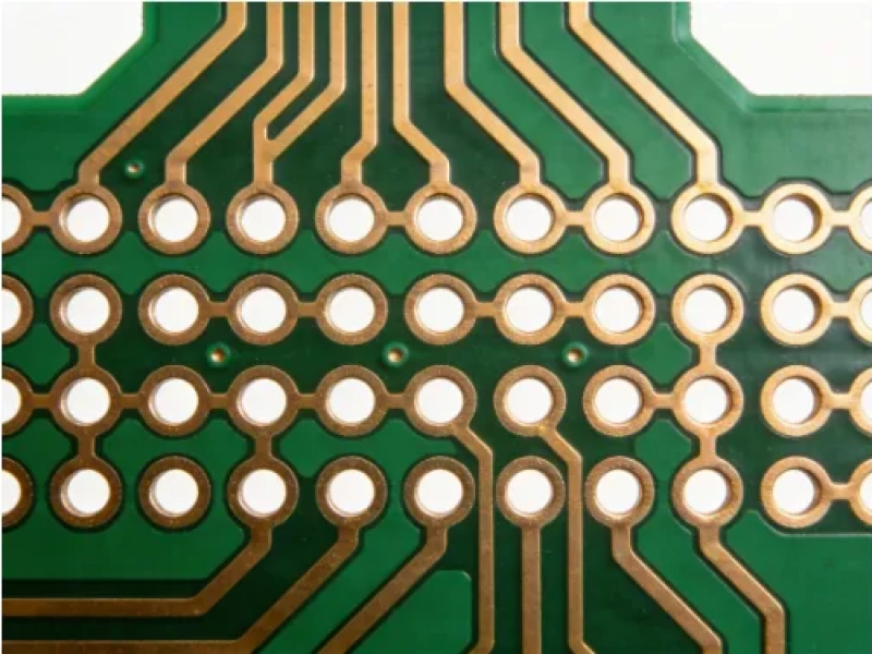
KnownPCB high-frequency PCB panel from its high-frequency and high-speed PCB page.
The surface artwork is only one part of this review. Add the layer names and the reference conductor for each RF section to the stackup or an associated note. Where the route changes from an external layer to an internal layer, identify both line structures and the ground connection between them. This gives the manufacturing review a specific set of features to check.
A microstrip has a signal strip above a reference plane, separated by dielectric. A stripline places the signal within the dielectric between reference conductors. Grounded coplanar routing adds ground copper alongside the surface strip. These are different electromagnetic structures, so a width established for one cannot simply be transferred to another.
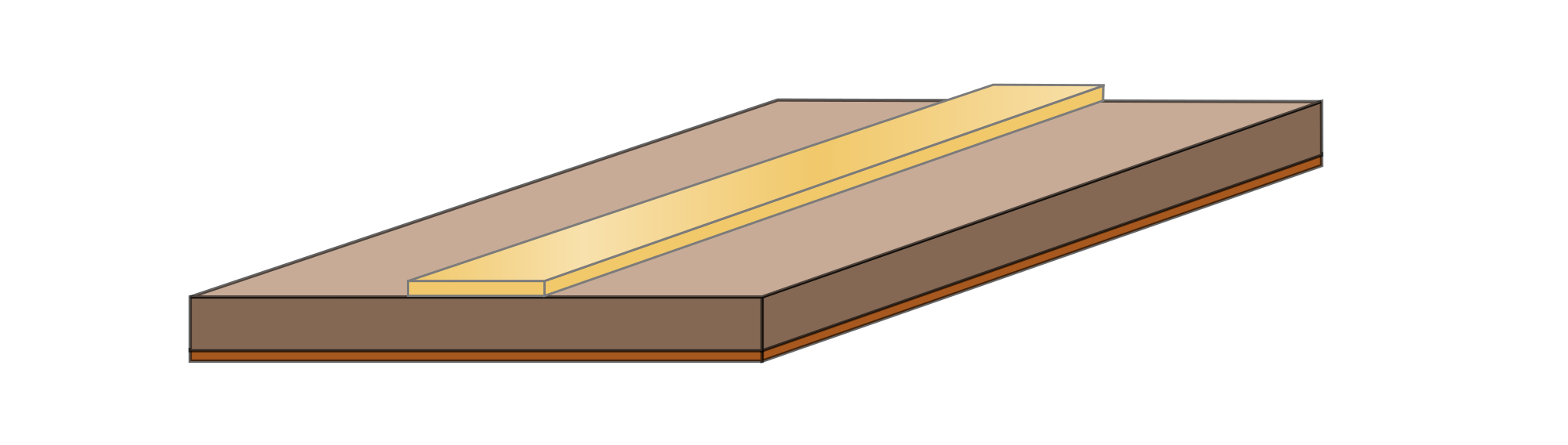
Microstrip structure diagram by Spinningspark, shared under CC BY-SA 3.0; original file.
The cross-section should include the local dielectric spacing, finished copper geometry and nearby ground. Overall board thickness does not identify the distance from the RF strip to its reference plane. On a coplanar route, the lateral gap is also part of the geometry; changing a ground-pour clearance can change the line even when its signal width stays fixed.
For a numerical illustration, Analog Devices' RF layout note lists two microstrip examples using a dielectric constant of 3.8 and 1.4 mil copper. A 6 mil dielectric with an 11.5 mil conductor is listed at 50.3 ohms; a 10 mil dielectric with a 20 mil conductor is listed at 50.0 ohms. Those published examples show why a target impedance alone does not determine a width. They are specific example constructions, not a default width pair for another material or stackup. See the note's RF transmission-line examples.
Altium's microstrip and stripline comparison explains the different field environments. For the manufacturing handoff, the practical consequence is to attach each controlled geometry to its own layer and reference structure. A single width called "RF width" is insufficient when the route uses more than one structure.
Keep the broader question of calculating, controlling and measuring impedance in the separate controlled-impedance manufacturing article. The remaining checks here concern the local RF structure that an impedance callout by itself cannot describe.
Top-side copper beside an RF line must have a defined connection to ground if it is intended to act as coplanar ground. Check the net assignment, the via connections and the copper remaining around each via. A visually continuous strip can contain an isolated island after a clearance rule, antipad or mechanical feature removes its connection.
The via-fence illustration shows the intended relationship: ground vias join the top-side ground strips to the lower ground plane. It does not prescribe a pitch. Choose the arrangement for the actual frequency range, stackup and surrounding geometry, then verify that it survives the fabricator's hole, registration and copper-clearance checks.
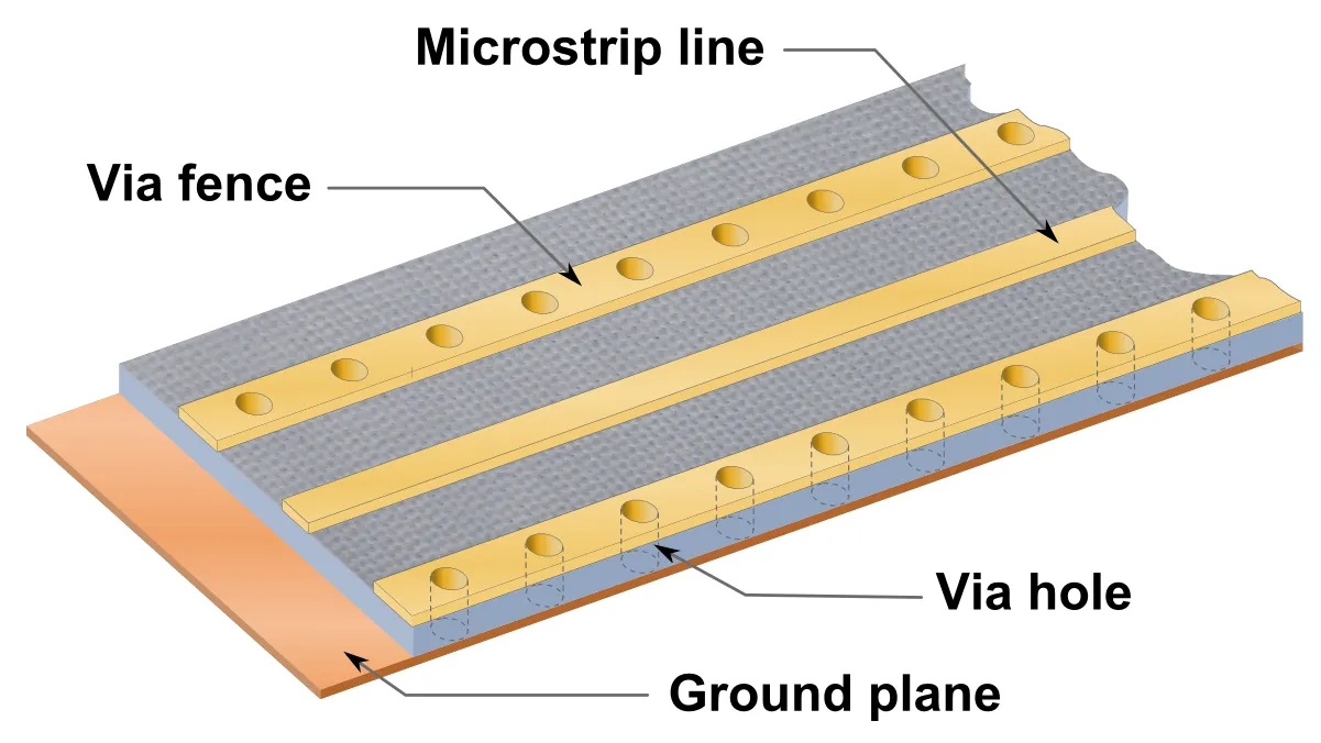
Via fence in microstrip, by Spinningspark, with background texture from Agnellous's public-domain Fibreglasscast.JPG. CC BY-SA 3.0; original diagram.
Review the spaces between signal features as well. Ground copper squeezed between two pads may disappear during a clearance update. A thermal-relief connection chosen for a soldered ground feature can differ from the solid connection intended by a component's RF layout guidance. Flag these local decisions in the source design so that a manufacturing query can be answered against the intended connection rather than against the apparent shape alone.
Increasing via count cannot repair a reference-plane slot directly under a route. Locate the actual return connection first. Also keep antenna and component keepouts separate from general stitching instructions; filling an intentionally empty RF region with ground vias can defeat the purpose of that region.
At a layer change, identify where the signal barrel connects and where the return current can move between reference conductors. Check the signal pad, clearance opening in each plane, nearby ground vias and unused barrel beyond the active connection. These features occupy the same small region and should be reviewed together.
TI's High-Speed Interface Layout Guidelines, in its ground-reference and via-discontinuity sections, explains the importance of maintaining the reference connection and limiting unused via stubs. Its interface-specific numerical recommendations should not be transplanted into every RF layout. Use the applicable device guidance and the actual RF structure when deciding which transition dimensions need analysis.
A useful drawing distinguishes the ground-stitching hole from the signal hole and names the connected layers. If a backdrill is required, give its entry side, protected connection and residual-stub definition. The separate backdrill residual-stub calculation covers that depth problem in detail. Keep this RF review focused on where the route and its return move.
Do not approve a transition solely because a uniform trace coupon meets its impedance target. The coupon can represent a straight transmission-line construction without reproducing the complete pad, barrel and reference change. Define any additional electrical evidence needed for the transition in the product verification plan, and confirm the measurement responsibility separately from bare-board fabrication.
At a device pad or connector launch, compare the actual land pattern with the reference design used by the circuit team. Check the stackup assumed by that reference, not only the footprint outline. The pad transition, nearby ground and opening in the reference plane can be intentional parts of the connection.
Separate the features the fabricator may compensate from those that require electrical approval. A long uniform strip may permit a reviewed width adjustment, while a short pad neck or connector gap may need to stay fixed. Identify those regions by layer and location. Otherwise a reasonable adjustment to meet one requirement can unintentionally change another feature.
This review stops at the fabrication interface. Connector-specific launch optimization belongs with the actual connector drawing and electrical model. The release package should preserve that approved geometry and describe any machining or board-edge requirements that affect it, without implying that the bare-board supplier has redesigned or validated the assembled RF interface.
| Review finding | What to identify in the files | Decision before release |
|---|---|---|
| A ground strip is separated from its vias | Ground net, clearance boundary and affected layer | Restore the intended connection or obtain electrical approval for a changed structure. |
| A route changes reference planes | Signal layer pair and return connection | Confirm how the reference conductors are connected near the transition. |
| CAM requests a width or gap adjustment | Uniform line sections versus protected pad or launch geometry | Approve the specific change against the released stackup. |
| A backdrill is added | Entry side, protected layer and residual-stub definition | Confirm the revised hole and depth data before fabrication. |
| Electrical verification is requested | Uniform-line coupon, transition structure or assembled interface | Assign the correct test object and responsible party. |
Close each query against one file revision. Retain the approved stackup, RF route locations and any marked restrictions on copper changes with the final fabrication package. If a material or construction change alters those assumptions, return the affected geometry for review rather than treating the old approval as transferable.
For a manufacturing review, send the stackup, RF material requirements, routing layers, controlled-geometry information and any local feature restrictions. KnownPCB's high-frequency and high-speed PCB manufacturing page provides the service context. Use the KnownPCB contact page to submit the board requirements and identify the RF features that need clarification before quotation or production release.
October/15/2026Stacked vs. Staggered Microvias: Choose by Constraint
September/12/2026High-current PCB Via Design Solution
November/03/2026HDI PCB Manufacturers in China: Comparison & 5 Key Checks
October/30/2026IPC Class 2 vs Class 3: Does Your 4-layer PCB Need a Redesign?
October/23/2026LED Aluminum PCB Dielectric: Voltage and Test Conditions
Proven by 7 industries, 4000+ customer projects
Please contact us at sales@knownpcb.com, ask for engineering support here or use the form below to reach out to KnownPCB | Request a Manufacturing QuoteInclude your quantity, target delivery date and key requirements. File handling and NDA information. |