Blog & Design Guide

A laminate datasheet says “breakdown voltage.” The lighting specification says “working voltage.” The purchase order asks for “high voltage aluminum PCB.” These statements do not define the same requirement. An LED aluminum PCB dielectric must be selected against the electrical stress and insulation function of the finished luminaire.
Start with the circuit-to-metal relationship. Determine which conductors can be energized, whether the metal base is accessible or bonded to chassis, and where insulation is needed. Only then compare materials and the conditions attached to their electrical data.
Contents
The dielectric beneath a copper circuit separates it from the aluminum base. Separation between two tracks on the same surface is another path, governed by the surface layout and environment. A slot or screw introduces more geometry. Selecting one dielectric value cannot resolve all these paths.
Draw the path from the energized copper to each relevant metal or accessible feature. Include the aluminum base, housing contact, fasteners, connectors, and any exposed board edge. Mark conductors that can move to a different potential during a fault or transient, according to the system design.
The LED package matters as well. Its thermal pad may be electrically isolated or tied to an electrical node, depending on the package. Read that package’s datasheet rather than assuming every thermal pad can be bonded to metal. A board insulation decision made from a generic LED symbol may be wrong for the selected part.
The existing LED aluminum PCB design-to-manufacturing article describes the broader construction. Here, keep the selection decision focused on the dielectric separating the circuit from aluminum and on the evidence needed to support that particular insulation function.
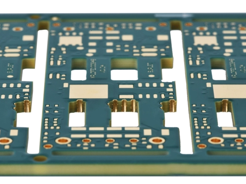
The aluminum PCB panel shown below provides product context. Its solder-mask colour and visible pad layout reveal neither the dielectric grade nor the electrical stress that the finished luminaire can withstand.
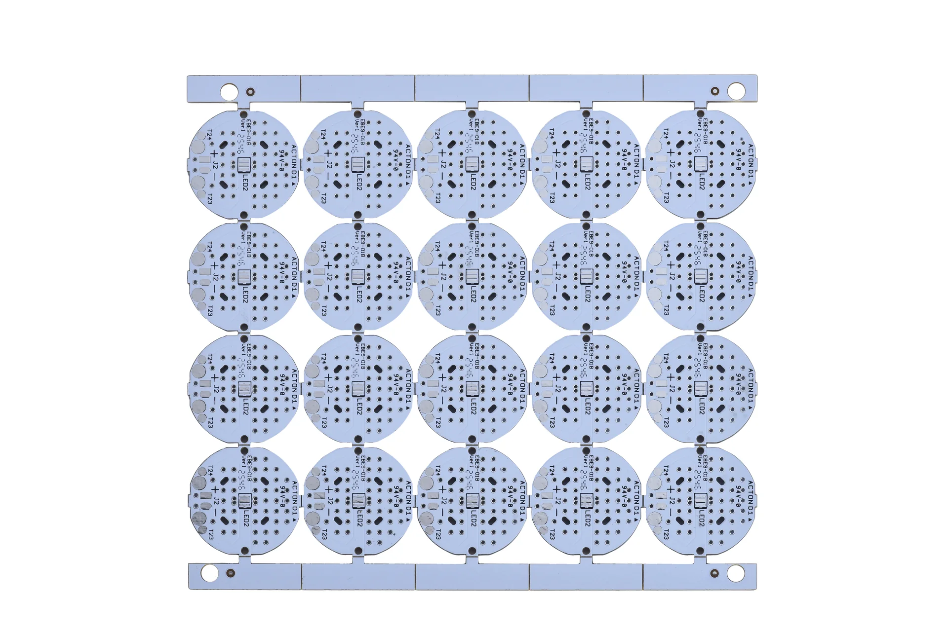
The photograph shows an aluminum-core PCB panel; its dielectric grade and voltage rating require separate specifications.
Breakdown testing drives a specimen to electrical failure under a defined method. A quoted result depends on specimen thickness, electrode arrangement, waveform, ramp or dwell, conditioning, and how failure is detected. A test on a flat material coupon is evidence about that specimen, not every possible finished-board feature.
A withstand test applies a specified stress for a specified time and evaluates whether the sample meets stated criteria. It has a different purpose from reporting the voltage at destructive breakdown. Neither label, on its own, defines the permitted continuous working voltage of the finished assembly.
| Term on a specification | What it describes | Information still needed |
|---|---|---|
| Breakdown voltage | Failure of a defined specimen under a test method | Material, thickness, electrodes, waveform and conditioning |
| Withstand requirement | A specified applied stress and pass/fail evaluation | Test duration, waveform, limits and responsible test party |
| Working voltage | Electrical stress in the intended product | The actual path, service conditions and applicable insulation design |
Henkel’s THERMAL CLAD selection document identifies electrical properties and the standards used to determine them, including ASTM D149 for dielectric breakdown. Use that method reference to ask comparable questions of candidate materials. Retain the exact grade and dielectric thickness with the reported value.
For an AC result, record whether the reported voltage is RMS and the test frequency. For a DC result, preserve that designation. Do not convert between AC and DC simply by relabelling a number. The product’s electrical design and applicable evaluation method determine the required stress.
Temperature and moisture conditioning deserve their own fields in the comparison. A dry room-temperature sample cannot establish performance at every service condition. Ask which data support the operating environment and which additional evaluation belongs to the product qualification plan.
Use a row for each proposed material and thickness. Record the supplier’s exact designation, data revision, nominal and permitted thickness, electrical property, method, and test conditions. Include whether the value is typical, a specified minimum, or an acceptance limit. A typical value is not automatically a purchase requirement.
Then add the system requirement separately. This should name the insulation path, working stress, relevant transient conditions, environment, and the product-level evaluation required by the responsible electrical designer. Keeping this row separate prevents a convenient catalogue value from becoming the design target without review.
Thermal performance is a second constraint on the same dielectric. A thinner layer may reduce through-plane thermal resistance while changing electrical margin and handling sensitivity. Compare candidates that meet the electrical requirement first, then evaluate the thermal path with the same component footprint and housing.
Mechanical features need attention before the material is frozen. Specify copper-to-edge geometry, holes, local machining, and any area where the metal is exposed. A good flat coupon result does not remove a burr, repair damage near a fastener, or insulate a copper feature that reaches an unintended metal surface.
Where a substitute is allowed, define the properties and documents that must remain equivalent. Matching thermal conductivity alone is insufficient. The dielectric grade, thickness, electrical data and processing compatibility must be reviewed together, and the engineering approval should precede production.
The KnownPCB metal-core PCB page treats insulation selection according to the construction and project conditions. Submit the actual dielectric and isolation requirements with the RFQ. Avoid copying an unqualified maximum-voltage statement into the purchase order as if it applied to every metal-core board.
Material identification supports traceability to the selected laminate. Dimensional inspection supports specified geometry. A netlist test supports circuit connectivity and isolation at the agreed test conditions. A product insulation evaluation has its own scope. State which document supports each requirement, and agree who performs any evaluation beyond the board supplier’s confirmed service.
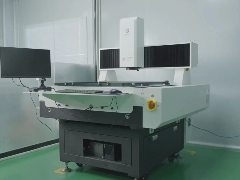
The electrical test fixture photograph below is included only to identify a bare-board inspection stage. It is not a photograph of a dielectric-withstand test, and it does not promise a high-voltage test report.
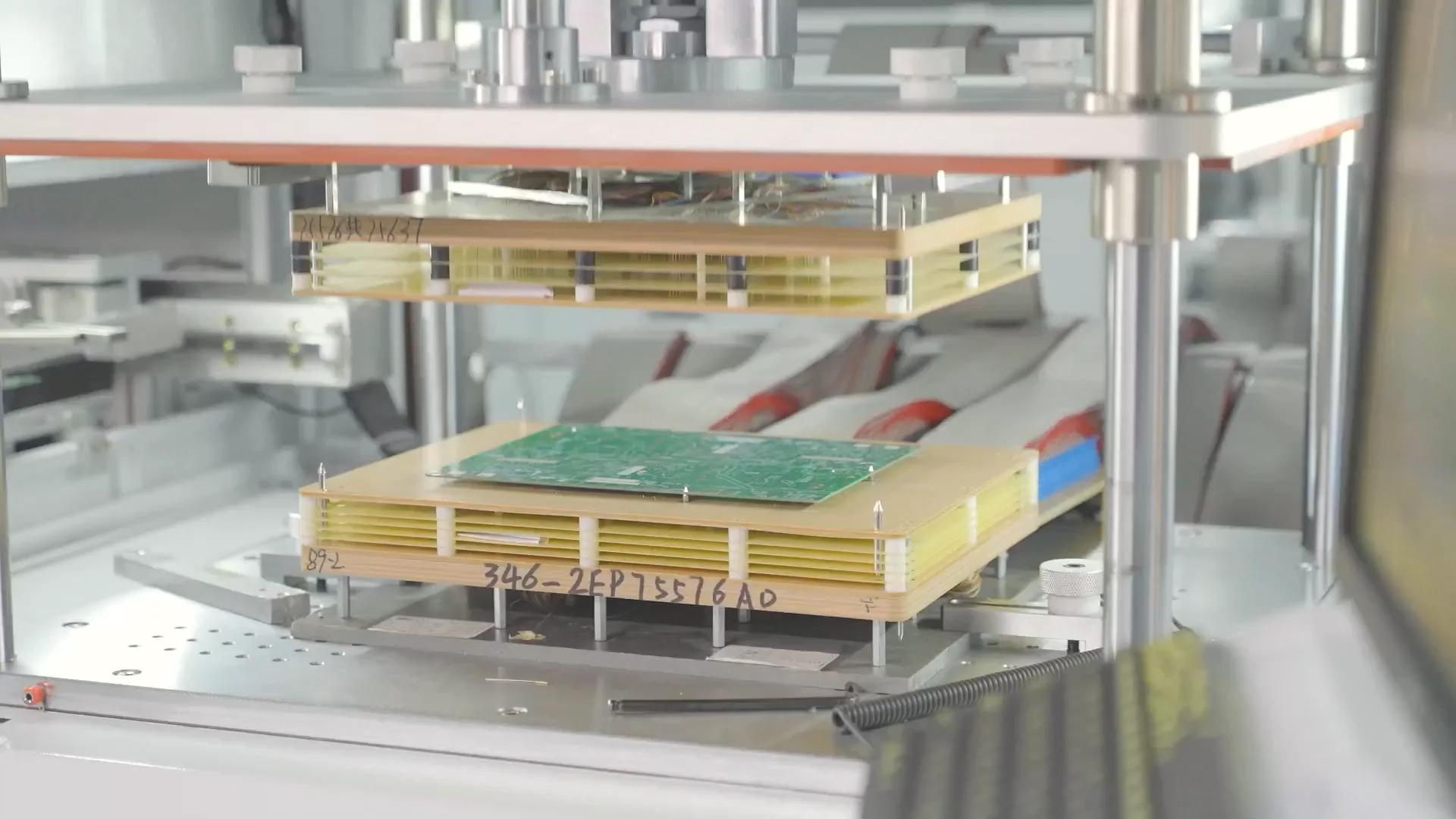
Bare-board electrical testing checks the agreed netlist; this image does not document a dielectric-withstand test.
Before approving the first production order, reconcile the material name on the quote, stackup, and fabrication drawing. Confirm that any test conditions in the contract are attainable and assigned to an identified party. If a requirement cannot be evidenced, resolve it before treating the construction as approved.
Preserve this record through revisions. Moving a mounting hole, enlarging a copper pour, or changing the housing interface can affect the insulation path even when the dielectric grade stays the same. The revision review should therefore cover the layout and mechanical changes as well as the material.
For a LED aluminum PCB material and DFM review, provide the circuit-to-metal diagram, dielectric datasheet, fabrication files, and required evaluation scope. These documents give the supplier a concrete construction to review while the product team retains responsibility for the luminaire’s electrical design and qualification.
Proven by 7 industries, 4000+ customer projects
Please contact us at sales@knownpcb.com, ask for engineering support here or use the form below to reach out to KnownPCB | Request a Manufacturing QuoteInclude your quantity, target delivery date and key requirements. File handling and NDA information. |